The board arrived from the fab house. Looked perfect. Then they tried to assemble it. The capacitor footprint was wrong. Off by 0.3mm. Doesn’t sound like much until you realize SMT assembly machines can’t place components on incorrect footprints. 500 boards. Completely useless.
The prototype worked flawlessly. Six months of firmware development. Ready for production. Then EMI testing. Failed spectacularly. Radiated emissions 40 dB over the limit. Why? Ground plane design that worked fine for one board became an antenna at production volumes. Complete PCB redesign required.
Battery life: 6 months promised. 3 weeks actual. The schematic showed a sleep mode circuit. But the PCB layout placed the pull-up resistor wrong, preventing the microcontroller from ever actually sleeping. Nobody caught it until after 2,000 boards were assembled.
These aren’t edge cases. These are the PCB design disasters we see regularly when teams treat circuit board design as pure electronics work and forget it’s also a mechanical, manufacturing, and production challenge.
According to IPC (Association Connecting Electronics Industries), PCB-related issues cause 35-45% of all product development delays in electronics manufacturing. Whether you’re building consumer products, industrial equipment, medical devices, or connected devices, the challenges are the same. Most issues trace back to decisions made during schematic and layout phases.
Custom PCB design isn’t just about making circuits work. It’s about making circuits that can be manufactured reliably, assembled efficiently, tested effectively, and perform consistently across thousands of units.
This guide explains how to design PCBs that survive the journey from schematic to production without expensive surprises.
When Do You Actually Need Custom PCB Design?
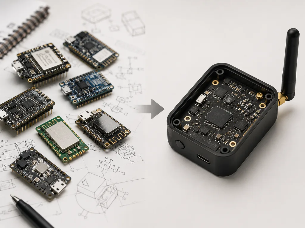
Let’s be honest about something most design firms won’t tell you: Not every product needs a custom PCB. Development boards and modules exist for good reasons.
Use Development Boards / Modules When:
- Volume under 100 units
- Still in prototype phase with changing requirements
- Need working prototype in 2-3 weeks
- Enclosure can accommodate larger boards
Need Custom PCB Design When:
- Volume 200+ units (custom PCB becomes cost-effective)
- Specific shape required to fit in enclosure
- Automated assembly needed at scale
- Precise power consumption requirements
- Long product lifecycle (5+ years)
Here’s where most teams go wrong: They jump straight to custom PCB because it feels “more professional” or they underestimate development time and cost. We’ve seen teams spend 6 months and significant investment on custom boards when a $40 ESP32 module would have worked fine for their first 500 units.
Pro tip: Start with modules for your first prototypes. Prove the product works. Get customer feedback. THEN design custom PCB when you know exactly what you need.
The 6 PCB Design Process That Prevents Failures
Most PCB design guides show you the steps. Here is where things actually go wrong at each step, because the consequences are real, not theoretical.
REQUIREMENTS → SCHEMATIC → COMPONENT SELECTION → LAYOUT → DFM REVIEW →
PROTOTYPE → TEST → REVISE → PRODUCTION
Phase 1: Requirements Definition (1-2 weeks)
Not just “what does it do” but:
- Power budget: How long must battery last? Exact current draw limits?
- Environmental: Operating temperature range? Humidity? Vibration?
- Mechanical constraints: Board size? Mounting holes? Keep-out zones?
- Production volume: This drives everything else
- Certifications needed: FCC? CE? UL? (Affects layout decisions)
Where teams fail here: They define features but not constraints. “We need WiFi and sensors” is not enough. You need: “WiFi module with sleep current under 10µA, operating -20°C to 60°C, fits in 45mm x 30mm space, assembled cost under $8 per board at 1,000 quantity.”
Phase 2: Schematic Design (2-4 weeks)
What it actually is: The logical connection diagram. Shows what connects to what, not where it goes.
- The schematic mistake that costs the most: Over-engineering. We see teams select microcontrollers with 10x the processing power needed because “it might be useful later.” Reality check: 80% of products with microcontrollers could run on a $2 chip. Most teams use an $8 one “just in case.” That’s $6 per unit. Multiply by 10,000 units. You just spent $60,000 on hypothetical future features.
Phase 3: Component Selection (Parallel with Schematic)
What you actually need to consider:
- Availability: Is it in stock at multiple distributors?
- Lead time: Can you get it in 2 weeks or 26 weeks?
- Lifecycle status: Is manufacturer still making it?
- Second source: Can you substitute if primary goes out of stock?
- Package: Can your assembly house handle it? (BGA requires X-ray inspection)
Here’s what happens when you ignore this: You design around a perfect component. Three months later, ready for production. Component is out of stock globally. 52-week lead time. You either wait a year, redesign the PCB, or pay 5x price to the grey market.
Phase 4: PCB Layout (3-6 weeks)
This is where theory meets reality. Where most failures actually originate. Covered in detail in the next section.
Phase 5: DFM Review (1 week)
Before sending to fabrication, experienced eyes review for manufacturability. What gets caught here: trace widths too small, hole sizes requiring special drill bits, silkscreen text too small to read, solder mask between pads too thin.
Phase 6-9: Prototype → Test → Revise → Validate
Budget for 2-3 PCB revisions. Teams that treat Revision 1 as “production ready” consistently end up with unusable boards in production.
Total realistic timeline: 16-24 weeks from requirements to production-ready boards.
→ Need a PCB designed right the first time?
Download our “PCB Development Checklist,” the exact 47-point review we use before sending any design to fabrication. Covers schematic, layout, DFM, and testing requirements.
Get the Free Checklist →
Schematic Design: Getting the Foundation Right
The schematic is your circuit’s blueprint. Mess this up and no amount of clever layout will save you.
- Power Supply Design: Where 60% of Problems Start
- The most common schematic mistake: Underestimating power supply requirements.
- Real example from our manufacturing floor: Client designed product with 3.3V linear regulator. Input: 12V. Current draw: 500mA steady state.
- Math: (12V – 3.3V) × 0.5A = 4.35W heat dissipation.
- Reality: LDO overheated in the plastic enclosure. Thermal shutdown. Product couldn’t run for more than 10 minutes.
- Fix: Switch to buck converter (switching regulator). Same output, 90% efficiency instead of 27.5%. Problem solved.
- Cost of the fix: 2-week delay, $3,500 in wasted boards, $4,200 for new prototype run. Cost if caught in schematic review: Zero. 30-minute conversation.
Protection Circuits: The Insurance Policy
- ESD Protection: Every exposed connector gets ESD protection. Period. Why: Humans build up static electricity. Touch your product. Zap. Thousands of volts. Without protection? Dead microcontroller. Cost: $0.15 per protection diode.
- Reverse Polarity Protection: If your product has a barrel jack or screw terminals, someone will plug it in backward. Simple protection: Series diode or P-FET. Cost: $0.30. Cost of not having it: Fried board. One-star reviews.
Schematic Review Meeting
- What we do: Schematic review meeting with PCB designer, firmware developer, assembly technician, and test engineer. 30-minute meeting. Catches 80% of problems before layout even starts.
4 PCB Layout: Where Most Teams Fail
Brutal truth: You can have a perfect schematic and still create a board that doesn’t work, can’t be assembled, or fails certification. Layout is where theoretical circuits meet physical reality.
Mistake 1: Ground Plane Disaster
- The rookie approach: Pour copper ground plane. Assume it’s all “ground” so it’s all the same.
- Why this fails: Digital circuits create high-frequency noise. Analog circuits need clean ground. Power circuits create voltage drop in ground. RF circuits need the ground plane as antenna counterpoise. If digital noise couples into analog ground, your ADC readings are garbage.
- Real example: IoT sensor with precision temperature measurement. Prototype worked perfectly.
- Production units: temperature readings jumped ±3°C randomly.
- Root cause: Ground plane layout. Digital MCU switching noise coupled into analog sensor ground through shared ground path.
- Fix: Star ground topology. Separate ground returns for analog and digital, joined at one point only.
Mistake 2: Power Supply Trace Width
Rule of thumb:
- 1A continuous: 0.5mm trace width minimum (internal layer)
- 3A continuous: 1.5mm trace width
- 5A+ continuous: Use power planes or very wide traces (3mm+)
What happens when you ignore this: Product works fine during testing. Goes into production. Extended operation. Trace heats up. Solder joint weakens. Eventually: open circuit. Intermittent failure. Nightmare to debug.
Mistake 3: EMI Layout Issues
- The expensive mistake: Designing layout without EMI in mind, then failing certification testing.
- Cost: FCC testing that fails = $15,000-$30,000 wasted. PCB redesign. Re-test. 8-12 week delay.
- Prevention: EMI-aware layout from the start. Pre-compliance testing with near-field probe during prototype phase.
Layout rules that prevent failures:
- Keep clock traces short, route on inner layers between ground planes
- Continuous ground plane, no splits
- Decouple caps within 2mm of IC power pins
- Series resistors near IC for IO traces
Mistake 4: Thermal Management in Layout
Heat needs to go somewhere. Poor thermal layout leads to thermal shutdown or reduced lifespan.
- Real example: IoT gateway with cellular modem. Power amplifier generates heat during transmission. Layout had minimal copper under PA. No thermal vias.
- Result: PA hit thermal limit during extended data upload. Throttled transmission. Data upload took 3x longer than expected. Battery drained faster.
Fix: Added 16 thermal vias under PA. Connected to bottom ground plane. Problem solved.
Cost if caught in layout: Zero. Cost after 1,000 boards manufactured: Can’t really fix. Poor product performance.
→ Building a wireless product? Get our RF layout guide
Free download: “RF PCB Layout Best Practices,” covers antenna placement, ground plane design, shielding, and the exact layout rules for WiFi, Bluetooth, and LoRa designs.
Download RF Layout Guide →
Design for Manufacturing (DFM) for PCBs
The gap that kills products: Beautiful PCB design that can’t be manufactured at scale.
DFM Rule 1: Design for Your Actual Assembly Process
The mistake: Designing for hand assembly, then trying to scale to automated. Doesn’t work.
Even for prototypes, design knowing automated assembly is the goal. This means:
- Component spacing for pick-and-place machines
- Fiducials on every panel
- Test points in consistent locations
- No components on bottom side if possible (single-pass assembly)
DFM Rule 2: Component Selection for Assembly
Real numbers from production floor:
- 0603 resistor assembly: $0.02 per component
- 0402 resistor assembly: $0.05 per component (smaller, harder to place)
- BGA assembly: $0.50 per component (requires X-ray inspection)
Multiply by thousands of components. Multiply by thousands of boards. Cost adds up fast.
DFM Rule 3: Panel Design
If producing more than 100 boards: You’re likely ordering panels. Panel design considerations:
- V-score or routed tabs: How do boards separate?
- Fiducials: Need global fiducials for panel alignment
- Board spacing: Enough space for depaneling
- Orientation: All boards same rotation for assembly
DFM Rule 4: Test Point Strategy
- The mistake: Adding test points as afterthought. They end up in inconvenient locations, hard to access, inconsistent spacing.
- What we do: Test point locations planned during layout. Test engineer reviews. “Can you actually build a fixture for this?” If no, adjust layout.
DFM Rule 5: Rework and Repair Consideration
Boards will fail. Components will need replacement. Plan for it.
Good DFM for rework: Component spacing allows soldering iron access, large components have thermal relief on ground planes, critical components not buried under other parts.
Component Selection Strategy
The component selection mistake that costs the most: Choosing parts based on specs and price alone, ignoring availability and lifecycle.
The Multi-Sourcing Rule
For every critical component, have 2 sources. Pin-compatible parts from different manufacturers allow you to swap without a PCB change if your primary source goes out of stock.
What we see regularly: Team designs around perfect component. Goes into production. Component out of stock. 26-week lead time. Project dies or faces massive delay.
What we do: Component selection review with purchasing team. They check: current stock, lead times, lifecycle status, second sources. This happens DURING schematic phase, not after layout is done.
Lead Time Management
The planning rule: Longest lead time component drives your production schedule.
Real example from our floor: Client needed 500 units. Custom MCU had 20-week lead time. We caught this during component selection. They ordered MCUs immediately. Design took 12 weeks. MCUs arrived week 16. Assembled week 17. Hit their deadline.
If we caught this AFTER design was complete? They would have missed deadline by 8 weeks.
Price at Volume
The BOM cost calculation mistake: Adding up single-unit prices and assuming that’s your cost.
Example:
- Product designed with $15 BOM at single-unit pricing. Looks expensive.
- Same product at 1,000 unit volume: $8.50 BOM. Totally different margin profile.
Testing and Validation
Bring-Up Testing
Basic bring-up sequence:
- Visual inspection before applying power
- Power supply check: Measure voltages without ICs installed
- Install ICs, test again
- Basic firmware: Load minimal code to toggle GPIO
- Peripheral testing: One by one, test each circuit
Time required: First board bring-up: 4-8 hours if design is good. Days if there are major issues.
Power Consumption Testing
For battery-powered products: critical.
The measurement challenge: Can’t use regular multimeter. Sleep currents in microamps. Need precision measurement.
Where teams fail: Assume sleep mode works based on datasheet. Don’t measure actual current.
Reality: Something preventing actual sleep. Pull-up resistor keeping circuit active. LED left on. Sensor polling when it shouldn’t be.
Result: Expected 6-month battery life. Actual 3 weeks.
EMI/EMC Testing
Pre-compliance testing: Before paying for official testing, test yourself.
If you wait: Official testing failure = expensive. PCB redesign. Re-test. Delay.
Production Test Planning
How will you test 1,000 boards efficiently?
Production test requirements:
- Speed: Each board should test in under 2 minutes
- Repeatability: Same test every time, no human judgment
- Coverage: Detect all likely failures
→ Ready for production? Get our test plan template
Free download: “PCB Production Test Plan Template,” covers test strategy, fixture requirements, programming setup, and quality control procedures.
Download Test Plan Template →
Production Transition
The valley where many products die: Prototype works. Production fails.
Production Pilot Run
Before ordering 1,000 boards, order 50-100.
What you’re testing:
- Assembly yield: Target more than 95% on first attempt
- Test yield: Target more than 98%
Real example from our floor: Client product looked great. Pilot run of 100 boards.
Assembly yield: 92%. 8% had solder bridges on QFN package.
Investigation: Reflow profile wasn’t optimal for that package. Adjusted temperature profile. Yield improved to 98%.
Cost: 2-week delay, $2,000 in reworked boards. Cost if discovered at 1,000 board run: 80 boards needing rework. Weeks of labor. Delay to customer.
Quality Control
The testing strategy:
- 100% visual inspection: Every board checked for obvious defects
- Sample X-ray: First, middle, and last board of production run
- 100% functional test: Every board powered up and tested
The math:
- Functional test cost: $2 per board
- Field failure cost: $50 per board (return shipping, replacement, labor, customer dissatisfaction)
- If 2% of boards are defective without testing on 1,000 boards: 20 failures in field, cost $1,000
- If you test all boards: $2,000 in testing, catch 20 defectives before shipping, fix in house at $5 per board = total $2,100. But you didn’t ship defective products.
5 Common PCB Design Mistakes (and How We Catch Them)
After manufacturing thousands of boards, these are the mistakes we see repeatedly:
Mistake 1: No UART/Debug Port Always include UART debug output. Even if “production version won’t need it.” Debugging during development saves weeks. And even production boards fail. Debug access is insurance.
Mistake 2: Forgetting Pull-Up/Pull-Down Resistors Without them: Input floats. Random noise toggles it. Unpredictable behavior.
Real impact: Board works on bench (because engineer touches it, body capacitance provides pull-up). Fails in enclosure (floating input toggles randomly).
Mistake 3: Missing Decoupling Capacitors Every IC power pin needs decoupling cap nearby. Not “on the board somewhere.” Right at the pin.
Symptoms without proper decoupling: Intermittent crashes, communication errors, ADC noise, reset issues. All hard to debug. All preventable.
Mistake 4: Ignoring Component Height The scenario: PCB fits in enclosure (barely). Tall components hit enclosure lid. Can’t close it.
Prevention: 3D model of PCB with component heights. Import into enclosure CAD. Verify clearance.
Mistake 5: Single Power Source for Everything Digital circuits, analog circuits, RF circuits all on same power supply. Digital switching noise couples into analog ground. Analog measurements garbage. RF performance poor.
Fix: Separate power domains. Filter between them. Ferrite beads, LC filters.
Where 80% of these mistakes come from: Working in isolation. No cross-functional review.
Every design gets reviewed by: PCB designer, firmware developer, test engineer, assembly technician, and manufacturing engineer. Each brings a different perspective. Each catches different problems.
30-minute review. Saves weeks of debugging and rework.
Frequently Asked Questions
How much does custom PCB design actually cost?
The real cost driver is the number of iterations. Good requirements and review process = 2-3 iterations. Poor requirements = 5-6 iterations.
At CADLETE we provide complete product development including PCB design, not separated line items. You get design, prototyping, iteration, and manufacturing coordination as an integrated service.
How long does PCB design actually take?
requirements to production-ready:
Simple board: 12-16 weeks (design, prototype, test, revise, validate)
Medium complexity: 16-20 weeks
Complex board: 20-24 weeks
The timeline trap: Teams expect 4-6 weeks. Reality hits when testing reveals issues needing another revision.
Can’t I just use an Arduino or Raspberry Pi instead?
Absolutely, and you should consider it.
When Arduino/Pi makes sense: Prototyping, low volume (under 100 units), time-to-market is critical.
When custom PCB makes sense: Volume above 200 units, size constraints, production scaling, long product life (5+ years).
The smart path: Prototype with development board. Validate concept. Prove market. THEN design custom PCB knowing exactly what you need.
What’s the difference between 2-layer and 4-layer PCBs?
2-layer: Top and bottom copper. Simpler, cheaper. 4-layer: Top, bottom, and 2 internal layers. Usually one internal ground plane, one internal power plane.
When you need 4-layer: High-speed signals (USB, Ethernet), EMI is a concern, complex routing, better power distribution needed.
Cost difference: 4-layer is typically 2-3x cost of 2-layer.
What certifications does my PCB need?
Depends on product and markets:
FCC (United States): Part 15 for unintentional radiators, Part 18 for intentional radiators
CE (Europe): EMC Directive, Low Voltage Directive, RoHS
UL (Safety): Electrical safety certification
When to think about it: During schematic and layout, not after boards are made.
Summary: The PCB Development Success Formula
- Start with Clear Requirements. Don’t just define “what it does.” Define power budget, size constraints, environmental conditions, volume, cost target.
- Design for Your Actual Manufacturing Process. Custom PCB for production needs different design than prototype. Plan for automated assembly from the start.
- Component Selection is Critical. Available parts matter more than perfect parts. Lead time and lifecycle trump specs.
- Layout is Where Theory Meets Reality. EMI, thermal, power distribution: these are core layout decisions, not afterthoughts.
- Test Early and Often. First prototype will have issues. Budget for 2-3 iterations. Test each thoroughly.
- Manufacturing Integration Prevents Disasters. When design team and manufacturing team work together from day one, integration problems get caught early.
The gap between “works in lab” and “works in production at scale” is where most hardware products fail.
→ Ready to design a PCB that actually works in production?
Send us your product requirements. We will give you a PCB development recommendation covering component selection, manufacturing method, certification path, and realistic timeline.
What we cover in a free consultation:
- ✅ Review of your product requirements
- ✅ Component selection guidance (availability, lifecycle, alternates)
- ✅ Manufacturing method recommendations
- ✅ Realistic timeline from schematic to production
- ✅ Honest assessment of technical risks
Visit Our Facility: We encourage potential clients to tour our design and manufacturing facility in Ahmedabad. See where your product will be designed, prototyped, and manufactured, all in one location.
Related Resources
Deep Dive Topics:
- PCB Design to Production: Complete Guide → Learn about schematic design, component selection, PCB layout best practices, and manufacturing preparation for custom electronics.
- Choosing Manufacturing Methods: 3D Printing vs Injection Molding vs CNC → Understand when to use each manufacturing method, cost implications, and volume considerations.
- Firmware Development for Smart Products → Explore microcontroller platforms, development workflows, and optimization techniques for embedded software.
- Design for Manufacturing: Electronics + Mechanical Best Practices → Detailed DFM guidelines for both mechanical and electronic aspects of product development.