
Choosing the Right Manufacturing Method: 3D Printing, Injection Molding, CNC Machining, or Die Casting
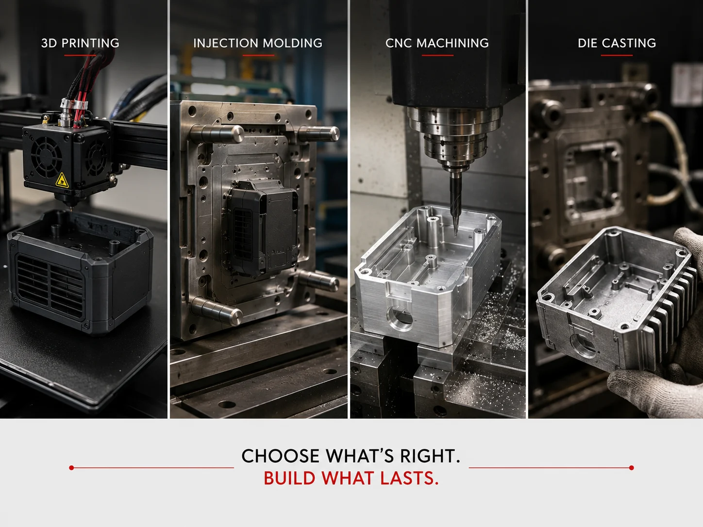
Most hardware teams choose a manufacturing method the same way: look at cost per unit, look at tooling cost, pick the one that fits the budget. That framework works until the product goes into production and something breaks.
The enclosure that looks perfect at $47 per printed unit costs $23,500 for 500 units. The injection-molded enclosure with $68,000 in tooling gets approved before the PCB layout is done, then the USB port does not align with the opening. The CNC-machined aluminum housing looks premium until the wireless range test comes back at 4 meters instead of 30.
These are not exotic failures. They are the predictable result of making manufacturing method decisions without the full picture. Volume and cost are only two of the variables that matter. Heat dissipation, RF transparency, assembly sequence, and PCB clearance determine whether the enclosure works with the electronics inside it, or against them.
This guide covers the complete decision framework across all five primary manufacturing methods, including the electronics integration factors that most manufacturing guides skip entirely.
Why This Decision Is More Complex Than It Looks
Every manufacturing guide compares methods on three dimensions: cost per unit, tooling cost, and lead time. Those matter. But they are not where teams run into serious trouble.
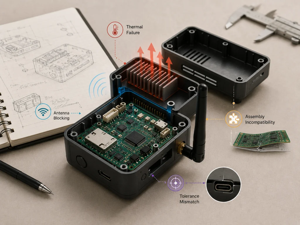
- Thermal failure: The enclosure material traps heat the electronics generate. The product hits thermal shutdown at 72°C. Nobody ran the numbers on heat dissipation during enclosure design.
- Antenna blocking: The material selected for aesthetics, brushed aluminum or die-cast zinc, shields the antenna. Wireless range drops from 30 meters to 3. The electronics team was not consulted when the housing material was chosen.
- Assembly incompatibility: The snap-fit enclosure requires an assembly sequence that makes PCB installation impossible without flexing the board past its limit. Caught on the production floor, after tooling is already paid for.
- Tolerance mismatch: The PCB was laid out to fit the 3D-printed prototype. The injection-molded production enclosure is 0.4mm tighter. The USB connector no longer aligns with the opening.
None of these are manufacturing problems in isolation. They are integration failures, the predictable result of making enclosure decisions without electronics team input. Research from Modus Advanced shows that approximately 70 percent of manufacturing costs are locked in during the design phase, before a single part is produced. The method you choose at the beginning determines what is and is not possible for everything that follows.
The sections below cover each method’s core specs and the electronics considerations that belong in every housing decision.
3D Printing: The Fastest Path to Learning
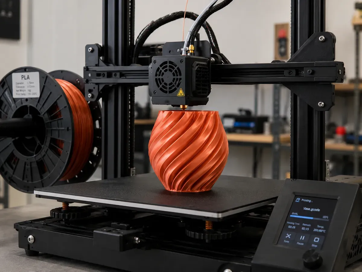
What it is: 3D printing builds parts layer by layer from a digital file with no tooling required. At CADLETE we operate three primary technologies, each with a different purpose.
- FDM (Fused Deposition Modeling): Extrudes thermoplastic filament layer by layer. Fastest and lowest cost. Surface finish shows layer lines. Best for functional prototypes and early concept validation.
- SLA (Stereolithography): Cures liquid resin with a UV laser. Excellent surface finish and fine detail. Best for appearance models, thin-walled geometry, and parts where a smooth surface matters without post-processing.
- MJF (Multi Jet Fusion): Fuses nylon powder with a thermal print head. Produces near-isotropic strength, meaning consistent mechanical properties in all directions. Best for functional enclosures in small production runs where tooling investment is not yet justified.
The 3D printing market reflects how central this technology has become to product development. According to Grand View Research, the global 3D printing market was valued at $30.55 billion in 2025 and is projected to reach $168.93 billion by 2033, growing at a CAGR of 23.9 percent. Prototyping remains the largest application segment, which aligns with exactly how we use it: learn fast before committing tooling spend.
When 3D Printing Is the Right Answer
- Volume under 100 to 200 units: No tooling cost, parts in 24 to 72 hours. This is where you discover what actually needs to change before spending on molds.
- Geometry that cannot be molded: Complex internal channels, undercuts, and organic forms that would require multi-piece molds or be impossible to demold. If you genuinely need that geometry in production, 3D printing may be the only viable path.
- Rapid iteration cycles: Design review Monday, physical part Thursday. The speed of feedback during early development is irreplaceable. Three prototype iterations with 3D printing versus three injection mold revisions: 8 weeks versus 18 months.
Electronics Integration: What to Know
- Thermal performance: Most 3D printing materials are poor thermal conductors. PLA softens around 60°C, PETG holds to around 80°C, standard ABS to approximately 100°C. MJF nylon handles heat better than FDM materials, but none of these are thermal management solutions for electronics generating meaningful heat. If your product has switching power supplies, motor drivers, or RF power amplifiers, thermal performance must be validated separately and not assumed to carry over from the 3D-printed prototype to the production enclosure.
- RF performance: 3D printing materials are RF-transparent. FDM, SLA, and MJF enclosures will not attenuate WiFi, Bluetooth, or cellular signals. This matters if you plan to transition to a metal manufacturing method later. What passes wireless testing in a 3D-printed enclosure will not automatically pass in aluminum.
- Dimensional accuracy: FDM typically holds tolerances of ±0.3 to 0.5mm. Sufficient for prototype verification that your PCB concept fits, but do not design your PCB layout to prototype tolerances if injection molding is the production intent. As covered in our PCB Design to Production guide, PCB-to-enclosure fit must be re-validated every time the manufacturing method changes.
- Where 3D printing misleads teams: It is too forgiving. No draft angles required. Thin walls that would fail injection molding look fine in a print. Teams gain false confidence heading into tooling. The correct approach: prototype in 3D printing, but design to production tolerances and DFM rules from the first CAD sketch.
Cost and lead time:
- Practical volume range: 1 to 200 units (FDM/SLA), up to 500 units (MJF for the right applications)
- Tooling cost: None
- Per-unit cost: $15 to $300+ depending on size, material, and technology
- Parts lead time: 1 to 5 days
Injection Molding: The Production Standard
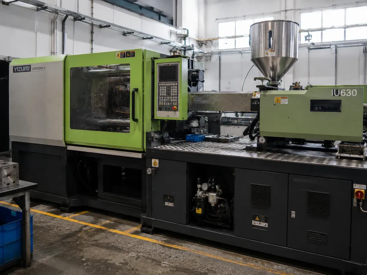
What it is: injection molding forces molten thermoplastic into a steel or aluminum mold under high pressure. The mold opens once the material cools and solidifies, releasing the finished part. The mold is reused tens of thousands to millions of times.
It is the dominant manufacturing method for plastic enclosures in consumer electronics, industrial equipment, and IoT products at commercial scale. According to Grand View Research, the global injection molding market was valued at approximately $299 billion in 2024, reflecting how foundational this process is across virtually every hardware industry. When designed correctly, injection molding delivers consistent geometry, excellent surface finish options, and low per-unit cost at volume.
When Injection Molding Is the Right Answer
- Volume above 500 to 1,000 units: This is the threshold where tooling cost begins to amortize meaningfully. A $15,000 mold spread across 10,000 units adds $1.50 per unit in tooling cost.
- Consumer products requiring finished aesthetics: Injection molding achieves surface qualities that 3D printing cannot: textured matte, high-gloss, soft-touch, and Class-A surfaces. If the enclosure is part of the product’s perceived quality, injection molding is the standard.
- Products with long production lifecycles: Hardware that will run for five or more years amortizes tooling cost well and benefits from the consistency injection molding delivers at scale.
- Complex integrated features: Snap fits, living hinges, integrated bosses for self-tapping screws, and structural ribs: injection molding produces all of these as single-part features. This is where part count reduction happens. According to CLEVR’s 2025 DFM guide, DFMA studies show average part count reductions of 54 percent when DFM principles are applied systematically, with corresponding reductions in assembly steps and production cost.
Electronics Integration: What to Know
- Thermal management is a design decision, not a retrofit: Plastic is a thermal insulator. Heat generated inside a plastic enclosure stays inside unless you design a path out. For products dissipating more than roughly 2W continuously, ventilation must be designed into the enclosure geometry, coordinated with the electronics team on component placement, before tooling is approved. This point deserves direct emphasis: modifying an injection mold after tooling is cut costs $5,000 to $30,000 for meaningful changes and is sometimes geometrically impossible. Design ventilation slots and thermal access points before the mold is made. Discovering thermal shutdown in production testing is one of the most expensive mistakes in hardware development.
- RF transparency: Standard thermoplastics including ABS, polycarbonate, and PC-ABS blends are RF-transparent. This is a meaningful advantage for wireless products. You can achieve aesthetically finished, high-quality enclosures without antenna shielding problems. For products with WiFi, Bluetooth, Zigbee, or cellular connectivity, injection-molded plastic provides the most design freedom for antenna placement and performance.
- Wall thickness and PCB clearance: Standard wall thickness for most thermoplastics runs 1.5 to 3mm. Consistent wall thickness prevents sink marks and warping. Draft angles of 1 to 3 degrees minimum are required for clean ejection. These constraints directly affect the internal volume available for the PCB and components. A 2mm wall thickness not accounted for in PCB layout can mean a connector that no longer reaches the opening. Enclosure wall stack-up and internal clearances must be coordinated between mechanical and electronics design before either team finalizes their files.
- Assembly sequence: How does the PCB get installed? The full sequence, board in, connectors through, cable routing, lid closure, must be modeled in CAD before tooling is approved. A common production floor discovery: the PCB must flex to clear an internal rib, cracking the board at a connector. Or a connector must be seated before the PCB, but the physical sequence makes that impossible.
Validating your enclosure design before committing to tooling? Our integrated design and prototyping process catches fit and assembly issues in 3D-printed and CNC prototypes before the mold is cut.
Cost and lead time:
- Tooling cost: $8,000 to $80,000+ depending on complexity, material (aluminum vs. steel), and cavity count
- Per-unit cost at 1,000 units: $3 to $25 depending on size and geometry
- Per-unit cost at 10,000 units: $1 to $8
- Tooling lead time: 4 to 8 weeks
- Practical volume range: 500 to millions
CNC Machining: Precision When It Counts
What it is: CNC machining removes material from a solid block using precision cutting tools controlled by computer. Our facility operates 3-axis and 5-axis CNC machining centers for both metal (aluminum, stainless steel, titanium) and engineering plastics (Delrin, PEEK, polycarbonate).
Where injection molding adds material to a shape, CNC subtracts it from a block. This fundamental difference makes CNC the method of choice for tight tolerances, metal parts, and geometries that cannot be molded.
When CNC Machining Is the Right Answer
- Precision metal enclosures: Medical devices, industrial instrumentation, test equipment: applications where dimensional tolerances of ±0.025mm matter and aluminum or stainless steel is the required material.
- Low-to-medium volume metal production: Before die casting becomes economical, CNC produces aluminum and steel enclosures at any quantity without tooling investment. One unit or one thousand.
- Prototypes requiring production material properties: If you need to validate thermal performance, structural behavior, or EMI shielding characteristics in the actual production material, you need a prototype made from that material. CNC delivers production-intent aluminum or stainless without tooling cost.
- Complex internal features: Precisely machined channels, threaded inserts, and tight-tolerance mating surfaces: features that casting cannot achieve at the required accuracy.
Electronics Integration: What to Know
RF shielding: feature or problem? This is the single most important electronics integration question with CNC metal enclosures, and it must be answered before the enclosure design is finalized.
A solid aluminum enclosure provides excellent EMI shielding. It prevents radiated emissions from escaping and keeps external interference from entering. This is genuinely valuable for products with motor controllers, switching power supplies, or high-frequency circuits that would otherwise fail emissions testing.
But that same shielding blocks your antenna. A WiFi antenna inside a closed aluminum box achieves 2 to 5 meters of range instead of 30. Cellular signals may not penetrate at all.
The solutions each have real tradeoffs:
- RF-transparent window: Machine a cutout in the metal enclosure and fill it with an injection-molded or 3D-printed plastic insert. Maintains metal aesthetics and structural integrity while allowing RF transmission. Requires the electronics team to confirm antenna placement before CNC programming. The window must align precisely with where the PCB puts the antenna.
- External antenna: Route a coaxial cable from the internal PCB to an external SMA connector. Functional but affects product aesthetics and adds a potential failure point.
- Plastic panels over antenna zones: Metal structural chassis with plastic panels covering antenna areas. Common in industrial equipment. Maintains structural integrity while providing RF transparency where needed.
The rule: if your product has wireless connectivity, the RF transparency decision must be made before the CNC program is written, not after parts are machined.
Thermal advantage: aluminum’s thermal conductivity of approximately 167 W/(m·K), compared to roughly 0.2 W/(m·K) for most plastics, makes the enclosure a legitimate thermal management tool, but only if the thermal path is designed in. This means PCB layout placing hot components against the enclosure wall, thermal interface material bridging the gap, and possibly machined features for direct thermal contact. The benefit does not happen automatically. Both teams need to design for it explicitly.
Grounding coordination: metal enclosures require explicit grounding decisions. Where do the PCB ground connections attach to the enclosure? Where are ground standoffs? This affects EMC performance and safety compliance and must be aligned between electronics and mechanical design before either file is finalized.
Cost and lead time:
- Tooling cost: None
- Per-unit cost (aluminum, medium complexity): $50 to $500 per enclosure at low volume
- Lead time: 1 to 3 weeks
- Practical volume range: 1 to 5,000 units (above this, die casting becomes more economical for metals)
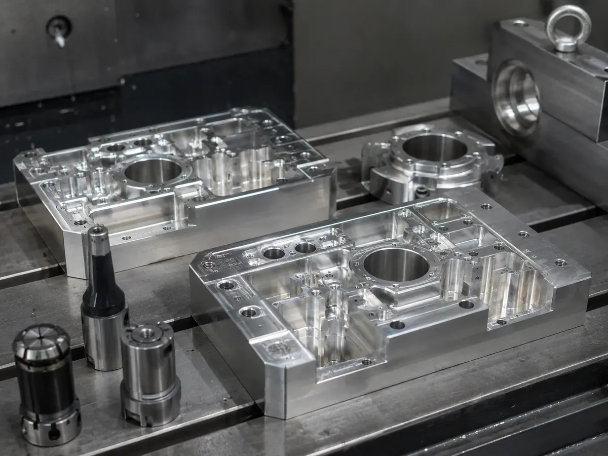
Die Casting: High-Volume Metal at Scale
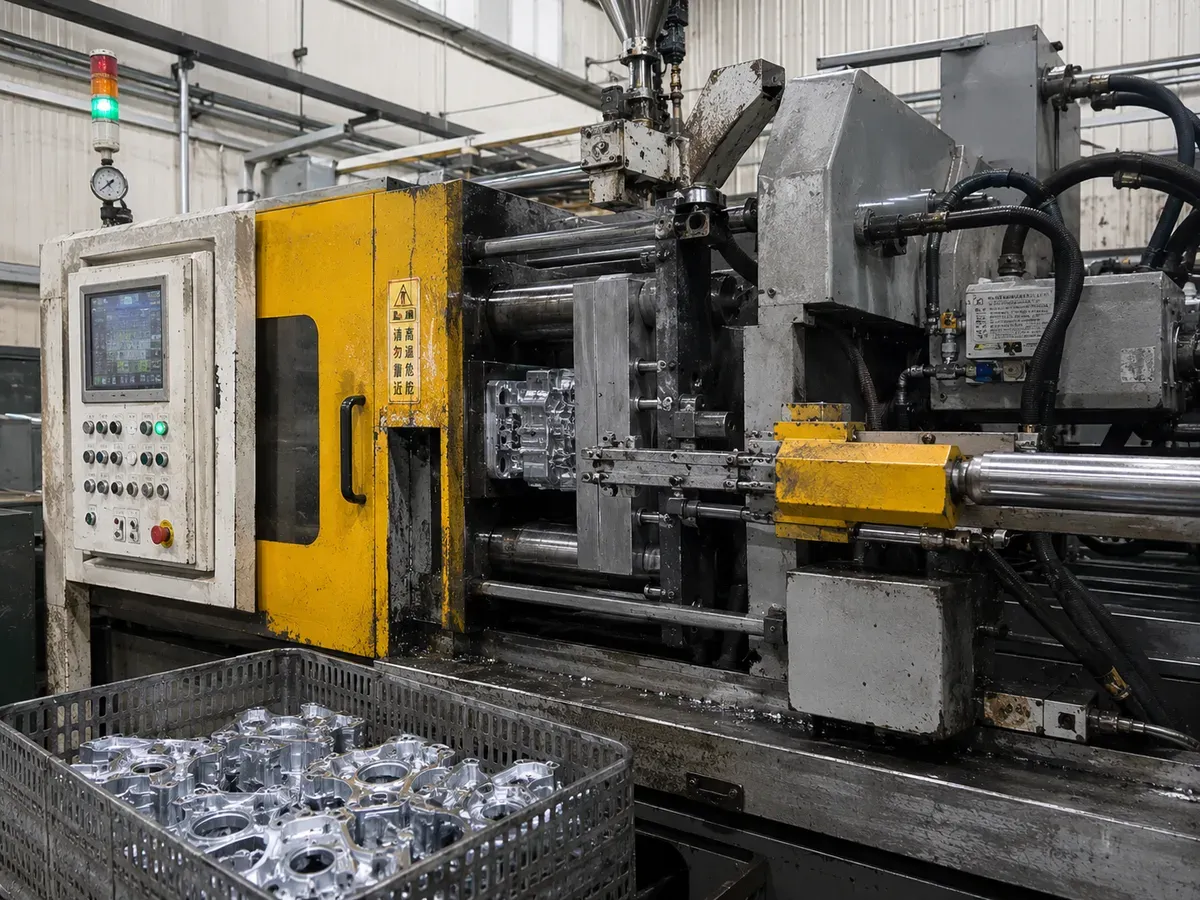
What it is: die casting forces molten metal, aluminum or zinc most commonly, into a hardened steel mold under high pressure. The mold opens once the metal solidifies, releasing a near-net-shape metal part. CADLETE operates die casting for both aluminum and zinc components.
Die casting combines the material properties of metal with the per-unit economics of injection molding, at the cost of significant upfront tooling investment.
When Die Casting Is the Right Answer
- High-volume metal enclosures: Above 5,000 to 10,000 units, die casting dramatically undercuts CNC machining on per-unit cost. At 50,000 units, a die-cast aluminum part that costs $4 per unit would cost $80 or more if machined from billet.
- Structural metal parts with complex three-dimensional geometry: Die casting handles shapes that would require extensive machining time if cut from solid stock. Cost stays low at scale regardless of geometric complexity.
- Products where metal is non-negotiable: Industrial equipment, automotive accessories, outdoor electronics: applications where plastic is not acceptable for environmental or mechanical reasons and volume justifies tooling.
Electronics Integration: What to Know
Die casting shares the RF challenge of CNC-machined metal enclosures, with one additional complication: tooling is expensive and has a long lead time. RF-transparent window decisions must be made before tooling is ordered, with electronics team confirmation on antenna placement, because modifying a die casting tool after the fact is significantly more costly than adjusting a CNC program.
Zinc versus aluminum for electronics enclosures: zinc die casting offers tighter tolerances and better surface finish but is denser and less thermally conductive than aluminum. For electronics enclosures where heat management matters, aluminum die casting is typically the right choice.
Post-machining for precision features: die casting typically requires secondary CNC operations for tight-tolerance features including threaded holes, precise mating surfaces, and connector openings. This is expected and should be factored into both cost modeling and lead time from the start.
Cost and lead time:
- Tooling cost: $15,000 to $100,000+
- Per-unit cost at 10,000 units: $4 to $20 for aluminum
- Tooling lead time: 6 to 10 weeks
- Practical volume range: 5,000 to millions
Sheet Metal Fabrication: Flat Geometry, Fast Turnaround
Sheet metal fabrication, laser cutting, press brake bending, and welding, produces enclosures and structural components from flat metal stock. At CADLETE this covers steel, aluminum, and stainless steel across all three operations.
When it makes sense: rectangular enclosures, chassis and frames, mounting brackets, industrial control panels. Geometry that works in a flat-then-bent form. Products where internal volume and cost efficiency matter more than organic shaping.
Electronics integration: steel sheet metal provides good to excellent EMI shielding. Aluminum sheet metal offers good thermal conductivity. Sealing for IP ratings happens at flanges and panel joints, which requires designed-in gasket grooves or foam tape sealing surfaces. Connector positions in the PCB layout must align with panel cutouts before laser cutting files are sent, a detail that requires mechanical and electronics coordination before fabrication, not after.
Cost and lead time:
- Tooling cost: Minimal to none
- Per-unit cost: $20 to $200 depending on complexity and material
- Lead time: 1 to 2 weeks
- Practical volume range: 1 to 10,000+ units
The Electronics Enclosure Decision Matrix
| Factor | 3D Printing | Injection Molding | CNC Machining | Die Casting | Sheet Metal |
|---|---|---|---|---|---|
| Volume sweet spot | 1 to 200 | 500 to millions | 1 to 5,000 | 5,000 to millions | 1 to 10,000+ |
| Tooling cost | None | $8K to $80K | None | $15K to $100K | Minimal |
| First parts lead time | 1 to 5 days | 6 to 10 weeks | 1 to 3 weeks | 8 to 12 weeks | 1 to 2 weeks |
| RF transparent | Yes | Yes | No (window needed) | No (window needed) | No |
| EMI shielding | No | No | Excellent | Excellent | Good to Excellent |
| Thermal conductivity | Poor | Poor | Excellent (Al) | Good (Al) | Good |
| IP rating achievable | With care | Yes | Yes | Yes | Yes |
| Typical tolerance | ±0.3 to 0.5mm | ±0.1 to 0.3mm | ±0.025 to 0.1mm | ±0.1 to 0.3mm | ±0.1 to 0.3mm |
| Surface finish quality | Fair to Good | Excellent | Excellent | Very Good | Good |
Five Questions to Answer Before Choosing
- 1. Does your product have wireless connectivity?: If yes, plastic methods are default compatible. Metal methods require an explicit RF window solution, and the electronics team must confirm antenna placement before the enclosure design is finalized.
- 2. What is the continuous thermal load from the electronics?: Under 1W, most methods work with care. 1 to 5W, ventilation must be designed into plastic enclosures; metal enclosures can conduct heat if the path is designed in. Over 5W, thermal management drives enclosure decisions and must involve both teams from the start, as covered in our End-to-End Product Development guide.
- 3. Does your product need to contain EMI?: Motor controllers, switching power supplies, high-frequency circuits: metal enclosure shielding addresses this directly. Factor the RF antenna tradeoff in explicitly when selecting metal.
- 4. What is your honest first-year production volume?: Overestimating volume to justify injection molding tooling is one of the most common and expensive mistakes in hardware development. If you are genuinely uncertain, 3D printing or CNC preserves optionality while demand is validated.
- 5. What is the full PCB installation sequence?: How does the board physically enter the enclosure? Which connectors need orientation access? Where do cables route? Model the complete assembly sequence in CAD before committing to any method with tooling cost.
Volume and Cost Crossovers
3D printing to injection molding: the financial crossover typically falls between 300 and 700 units. At this volume, per-unit savings from injection molding begin to pay back tooling cost over a reasonable product life. The design-stability trigger often comes first. Most teams move to injection molding when the design is locked and market demand is confirmed, regardless of whether the pure volume crossover has been reached.
CNC machining to die casting (metal parts): typically 3,000 to 8,000 units. Die casting’s per-unit advantage over CNC becomes compelling at scale, but the higher tooling investment requires enough volume to amortize. Under this threshold, CNC machining is almost always the right call for metal enclosures.
The cost modeling mistake teams make: calculating crossover on part cost alone. The full picture includes assembly time differences between methods, scrap and rework rates, test yield, and supply chain complexity. A part that takes 3 minutes to assemble versus one that takes 30 seconds can shift the economics entirely, independent of the per-unit material cost.
The Mistakes That Cost the Most
Choosing a method based on the prototype, not the production intent. 3D printing is the right prototyping tool. It is often not the right production tool. Designing to 3D printing’s design freedoms (no draft angles, thin walls, no mold flow consideration) and then transitioning to injection molding creates expensive surprises. Design to the production method’s rules from day one, even while prototyping in a different method.
Here’s the mistake we see constantly: teams optimize the prototype to work perfectly, then try to figure out manufacturing later. By that point, they are locked into enclosure geometries that require expensive mold modifications, tolerances that do not match the production process, and assembly sequences that nobody modeled. World-class product teams think about manufacturing from the first CAD sketch. Every enclosure design decision asks: can this be made efficiently at the volume we are targeting?
Selecting metal for aesthetics without resolving the RF problem. Brushed aluminum looks premium. Die-cast zinc looks industrial and durable. Both block the antenna if the enclosure is fully sealed in metal. If you select a metal method for aesthetic reasons and your product has wireless connectivity, the RF transparency solution must be explicit and confirmed by the electronics team before tooling is ordered, not discovered during wireless range testing.
Approving tooling before electronics layout is complete. The injection mold or die casting tool defines the enclosure geometry. If the PCB layout changes after tooling is ordered (a connector moved, a component is taller than expected, a heat sink needs to be added) the mold may need costly modification or full replacement. The correct sequence: complete PCB layout, verify mechanical fit in a shared 3D model, then approve tooling. Our PCB Design to Production guide walks through exactly why this sequence matters and where teams most commonly break it.
Ignoring thermal performance in plastic enclosures. Plastic enclosures work fine until extended operation in elevated ambient temperature. Run a worst-case thermal analysis covering maximum ambient temperature, maximum electronics power dissipation, and minimum ventilation, before the mold is cut. The cost of this analysis is hours. The cost of a mold modification after the fact is weeks and significant tooling spend.
Treating manufacturing method selection as a mechanical-only decision. This is the root cause underneath all the mistakes above. Manufacturing method selection affects RF performance, thermal management, grounding strategy, PCB clearance, and assembly sequence. All of these require electronics team input. If the electronics team is not in the room when the housing method is selected, integration problems are not a risk. They are a certainty.
Frequently Asked Questions
When should I switch from 3D printing to injection molding?
The financial crossover is typically 300 to 700 units, but the practical trigger is usually design stability plus validated demand. Ordering tooling on an unvalidated design is riskier than continuing to pay higher per-unit costs for another few hundred 3D-printed units while confirming product-market fit. Once the design is locked and the product is selling, tooling becomes the right move.
Can I achieve EMI shielding with an injection-molded plastic enclosure?
Yes, through two main approaches. Conductive coatings, copper or nickel applied inside the enclosure after molding, add EMI shielding to plastic parts. This is used regularly in mobile devices and medical equipment. Alternatively, internal metal shielding cans on the PCB contain emissions at the board level without requiring a metal enclosure. Both approaches add cost and process steps but preserve RF transparency for antenna zones.
What draft angle do injection-molded parts need?
Minimum 1 degree for smooth surfaces, 2 to 3 degrees for textured surfaces, up to 5 degrees for deep ribs or complex internal features. Zero-draft walls cause ejection problems: parts stick in the mold, surfaces drag during ejection, and tooling wears faster. Draft angles need to be in the CAD model from the start, not retrofitted during mold design.
Does CNC-machined aluminum actually help with electronics heat dissipation?
Significantly, but only if the thermal path is designed in. Aluminum’s thermal conductivity of approximately 167 W/(m·K) is roughly 800 times higher than typical plastics. But heat transfer from a hot component to the aluminum enclosure requires deliberate design: hot component placement adjacent to the enclosure wall, thermal interface material bridging the gap, and often machined standoffs for direct thermal contact. Assuming an aluminum enclosure will passively solve heat problems without designing the path is a common and costly mistake.
Die casting or CNC machining for aluminum enclosures, which is better?
It depends on volume and design stability. Under 3,000 to 5,000 units: CNC machining, with no tooling cost, faster lead time, tighter tolerances, and easy design changes if needed. Above 5,000 units with a stable design: die casting’s per-unit cost advantage becomes the deciding factor. Die casting also handles geometric complexity at no additional per-unit cost, a real advantage for enclosures with complex three-dimensional shapes that would be expensive to machine.
Can I combine manufacturing methods in one product?
Yes, and it is often the optimal answer. A common combination: an injection-molded plastic outer shell with a CNC-machined aluminum internal chassis. The plastic outer enclosure gives you RF transparency for antenna placement and good surface aesthetics. The aluminum chassis gives structural rigidity, a thermal path for hot components, and EMI shielding where needed. Method mixing adds supply chain coordination but lets each element of the product be optimized for its specific requirements.
How do I achieve an IP67 rating with injection molding?
IP67, dust tight and immersible to 1 meter, requires a continuous gasket groove with the correct compression ratio, no exposed fasteners that create leak paths, sealed or absent external connectors, and bonded enclosure halves through ultrasonic welding or structural adhesive. The PCB must have adequate clearance for gasket compression, and no sharp PCB edges that can cut the gasket over time. All of this is design work that happens during enclosure development. None of it can be added meaningfully after the mold is cut.
Summary: Key Takeaways
No single manufacturing method is universally correct. The right answer depends on volume, material requirements, electronics integration needs, and cost targets specific to your product.
Start with volume. This narrows the field immediately.
Then run the electronics questions: wireless connectivity, thermal load, and EMI containment requirement. These factors can override the default volume-based recommendation and must involve both the mechanical and electronics teams.
Then commit and integrate: the enclosure geometry and the PCB layout are not independent decisions. Every integration point including thermal path, antenna placement, connector alignment, and assembly sequence requires mechanical and electronics input before either team finalizes their files.
The most important principle in this entire guide: manufacturing method selection is not the last step in mechanical design. It is one of the first. Every design decision that follows flows from it. Lock it early, with all disciplines in the room.
Here’s the reality most development teams learn too late: the cost of fixing an integration problem doubles with each stage you progress. Catching a material-antenna conflict during design review costs hours. Discovering it after tooling is ordered costs tens of thousands and months of delay.
Early manufacturing decisions made with cross-discipline input are not about being thorough. They are about being profitable.
Get a Free Manufacturing Method Recommendation
Send us your product concept and requirements. We will give you a manufacturing method recommendation based on your specific volume, electronics requirements, and geometry, with realistic tooling costs, lead times, and DFM considerations for your actual design.
What we cover in a free consultation: manufacturing method recommendation for your product type and volume, electronics integration requirements for your enclosure (RF, thermal, EMI), realistic tooling cost and lead time for your geometry, a DFM review of your existing concept or early CAD, and an honest assessment of what is feasible and what is not.
Visit our facility: we encourage potential clients to tour our design and manufacturing facility in Ahmedabad. See the 3D printing, injection molding, CNC machining, die casting, sheet metal, and PCB assembly operations that support every product we develop, all under one roof.