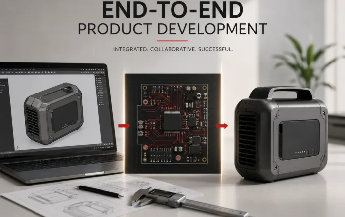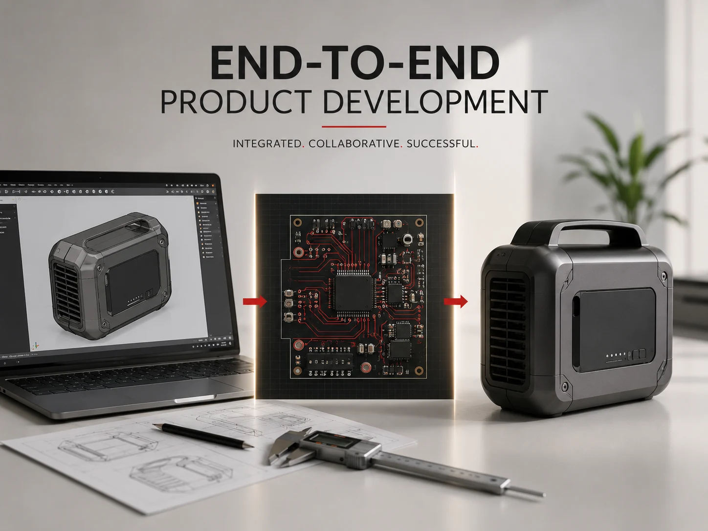
The PCB didn’t fit inside the enclosure. Off by 8mm. The industrial designer and electronics engineer had never spoken during the design phase. Result: Complete enclosure redesign. Four months wasted.
The product overheated in testing. The beautiful plastic enclosure had zero ventilation. The electronics generated heat nobody accounted for. Thermal shutdown at 85°C. Back to CAD modeling.
WiFi performance was terrible. Range: 3 meters instead of 30. Why? Metal enclosure parts blocking the antenna. The mechanical team didn’t know where the antenna was. The electronics team didn’t know the enclosure would be metal.
These aren’t hypothetical scenarios. These are real disasters we’ve seen repeatedly in product development when mechanical design and electronics engineering happen in silos.
Whether you’re developing consumer electronics, industrial equipment, medical devices, or IoT products, the challenge is the same: developing products that combine physical hardware with electronics and firmware requires a fundamentally different approach than traditional product development.
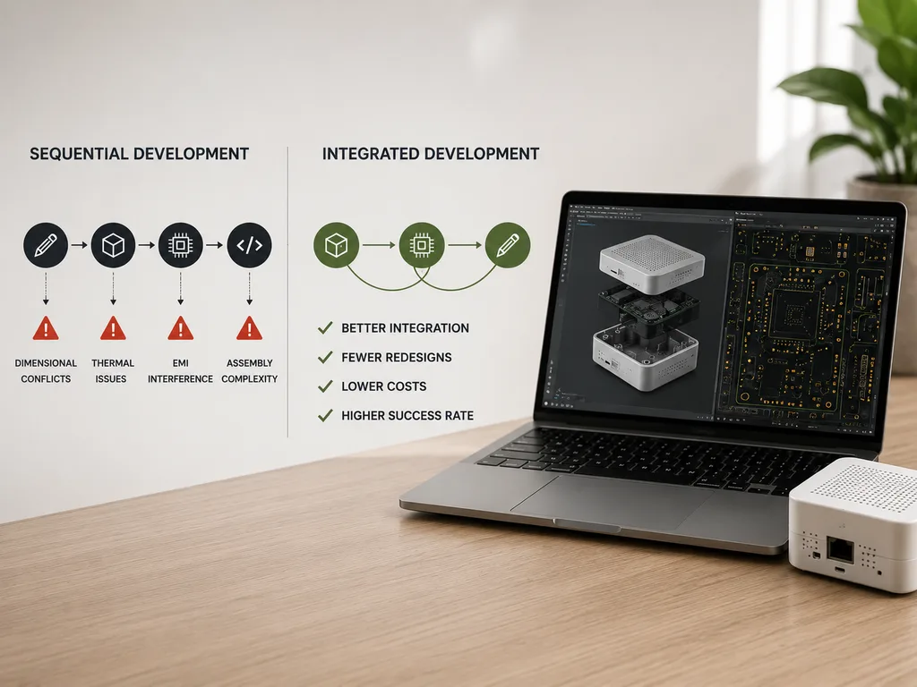
Sequential development (design → engineer → add electronics → write firmware) creates expensive problems. Integrated development (all disciplines working simultaneously) prevents them.
This guide explains exactly how to integrate mechanical design, electronics engineering, and firmware development from day one to avoid the costly mistakes that kill product launches.
What is End-to-End Product Development?
Quick definition: End-to-end product development for smart products means integrating mechanical design, electronics engineering, and firmware development from initial concept through manufacturing, with all disciplines working simultaneously, not sequentially.
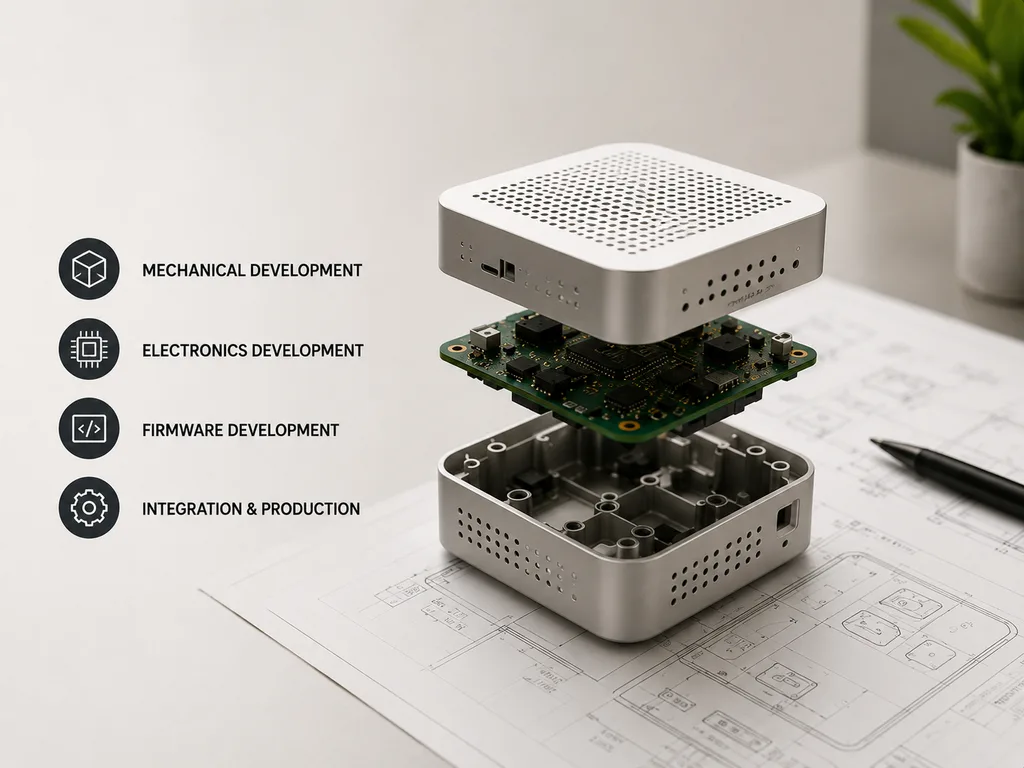
End-to-end product development encompasses the complete process of transforming a product concept into manufactured units ready for market. For smart products, this includes:
Mechanical Development:
- Industrial design and aesthetics
- CAD modeling and engineering
- Material selection
- Structural analysis
- Manufacturability planning
Electronics Development:
- Circuit design and schematic creation
- PCB layout and optimization (learn more in our complete PCB design guide)
- Component selection
- Power management systems
- Testing and validation
Firmware Development:
- Embedded software architecture
- Sensor integration and processing
- Communication protocols
- User interface programming
- Power optimization code (critical for battery-powered devices, see our firmware development guide for platform selection)
Integration and Production:
- System-level testing
- Regulatory certification
- Manufacturing setup
- Quality control systems
Why Mechanical + Electronics Integration Matters
The integration of mechanical and electronics design isn’t just best practice. It’s essential for product success in today’s market.
The Integration Challenge
Traditional product development follows a sequential process:
- Industrial designer creates the look
- Mechanical engineer makes it buildable
- Electronics engineer fits circuits inside
- Firmware developer writes the code
This approach creates problems that become expensive to fix later. Many of these issues stem from the lack of coordination between mechanical and electronics teams during the critical design phase.
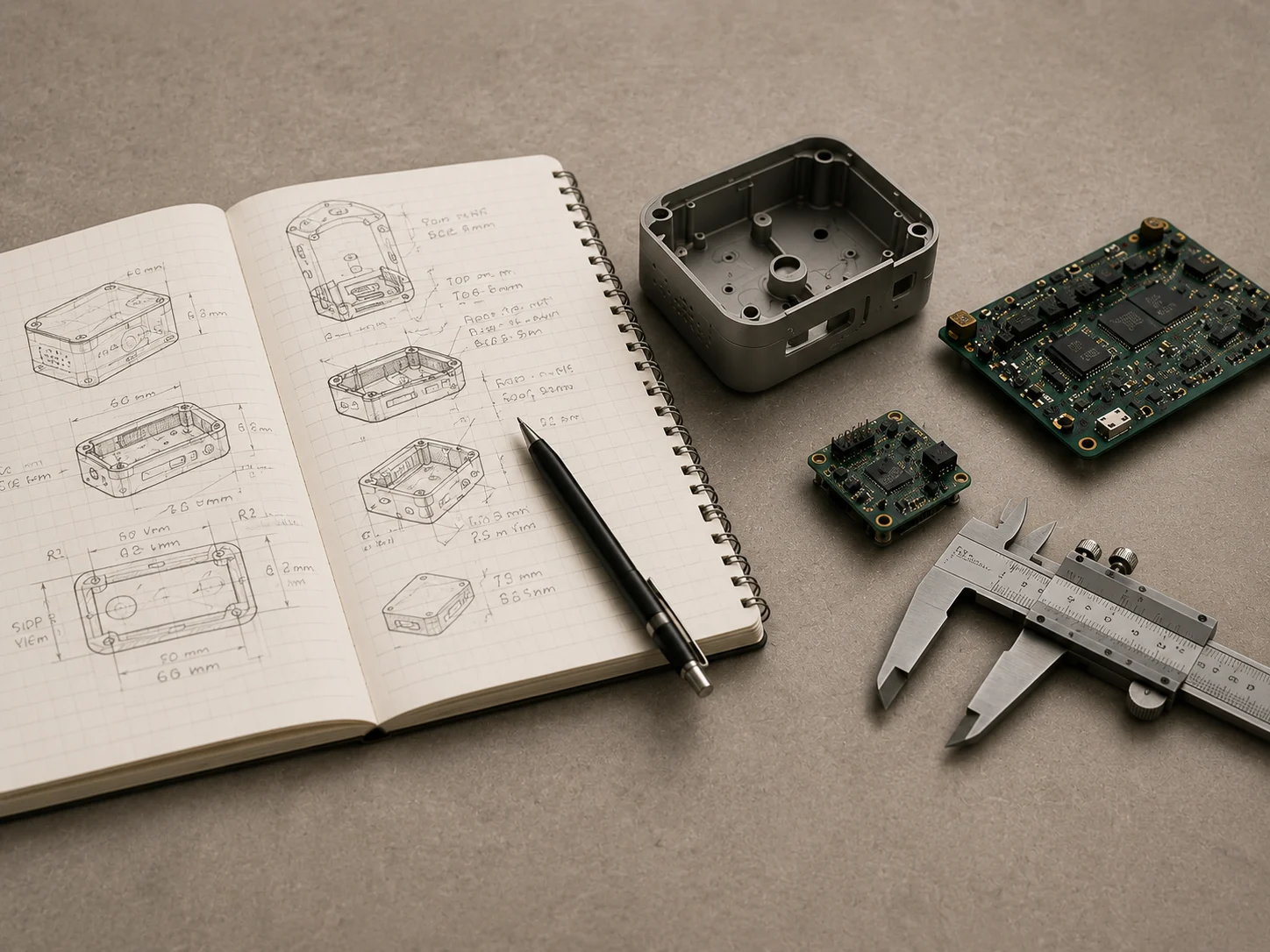
Problem 1: Dimensional Conflicts The PCB doesn’t fit inside the designed enclosure, requiring redesign of either the electronics or the enclosure.
Problem 2: Thermal Issues Electronics generate heat that the mechanical design doesn’t account for, causing performance problems or component failure.
Problem 3: EMI Interference Mechanical design choices (metal parts, enclosure gaps) create electromagnetic interference that affects electronic performance.
Problem 4: Assembly Complexity Designs that look good and function well electronically may be extremely difficult or expensive to assemble in production.
The Integrated Approach
Simultaneous development with cross-discipline collaboration solves these issues:
- Mechanical constraints inform PCB size and shape from day one
- Thermal requirements influence enclosure design and material selection
- Antenna placement is coordinated between electronics and mechanical teams
- Assembly methods are considered during initial design phases
Impact: Research from McKinsey’s Business Value of Design study shows that companies with integrated design practices achieve 32% higher revenue growth and 56% higher shareholder returns compared to industry peers. Additionally, data from the Product Development and Management Association reveals that best-performing companies achieve 76% product success rates, while companies using traditional sequential approaches manage only 51%.
Here’s the reality most development teams learn too late: The cost of fixing an integration problem doubles with each stage you progress. Catching a PCB-enclosure fit issue during design review costs hours. Discovering it after injection mold tooling is made costs tens of thousands and months of delay.
Early integration isn’t just faster. It’s the difference between profitable products and expensive failures.
From CAD to Your Doorstep: Complete Product Development + Manufacturing
We don’t just design your product and hand you files. We design it, prototype it, manufacture it, and ship it to you, all under one roof.
Free consultation includes:
- Integration risk assessment for your product concept
- Manufacturing method recommendations based on your volume
- Realistic timeline with our in-house production capabilities
The Product Development Framework
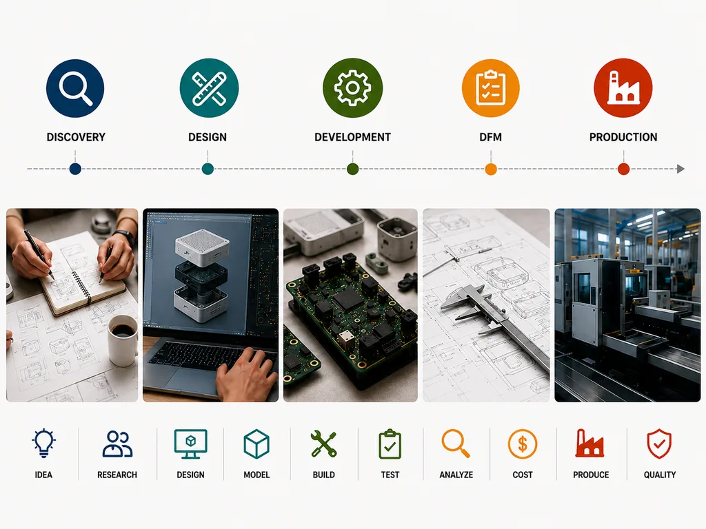
Smart product development follows this framework:
DISCOVERY → DESIGN → DEVELOPMENT → VALIDATION → PRODUCTION
    ↓           ↓           ↓             ↓            ↓
 Research    Integrate   Prototype    Test/Cert    Manufacture
Phase 1: Discovery and Concept (2-4 weeks)
Objectives:
- Validate market need and user requirements
- Assess technical feasibility
- Define feature scope and priorities
- Establish budget and timeline constraints
Key Activities:
- Market research and competitive analysis
- Technical risk assessment
- Initial architecture decisions (microcontroller platform, power source, connectivity)
- Rough cost modeling
Deliverables:
- Product requirements document
- Technical feasibility report
- Preliminary architecture diagram
- Project timeline and budget estimate
Phase 2: Integrated Design (6-10 weeks)
This is where mechanical and electronics teams work simultaneously.
Industrial Design Stream:
- Concept sketching and ideation
- 3D visualization and rendering
- User interface design
- Ergonomics and usability planning
Mechanical Engineering Stream:
- CAD modeling (SolidWorks, Fusion 360)
- Structural analysis and simulation
- Material selection and sourcing
- DFM preliminary assessment
Electronics Engineering Stream:
- Schematic design
- Component selection and BOM creation
- PCB layout planning
- Power budget calculations
Critical Integration Points:
| Design Element | Mechanical Consideration | Electronics Consideration |
|---|---|---|
| Enclosure dimensions | Aesthetics, ergonomics | PCB size, component height |
| Button placement | User interface, tactile feel | Switch type, board layout |
| Display integration | Viewing angle, protection | Connector routing, backlight |
| Battery compartment | Access, safety, size | Capacity requirements, charging |
| Ventilation | Appearance, water resistance | Thermal dissipation needs |
| Material choice | Aesthetics, durability, cost | RF transparency, heat conduction |
Deliverables:
- Approved industrial design (3D renders)
- Complete CAD assembly
- PCB schematic and layout
- Integrated BOM (mechanical + electronic parts)
Phase 3: Development and Prototyping (8-12 weeks)
Firmware Development (parallel stream):
- Algorithm development on dev boards
- Sensor integration and calibration
- Communication protocol implementation
- Power management optimization
- User interface programming
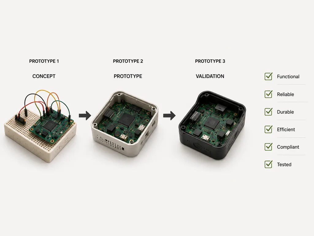
Prototype Progression:
Prototype 1: Proof of Concept (PoC)
- Purpose: Validate core technology
- Build method: Breadboard electronics + rough 3D printed enclosure
- Testing: Basic functionality only
- Timeline: 2-3 weeks
Prototype 2: Functional Prototype
- Purpose: Full system integration testing
- Build method: First PCB revision + refined 3D prints
- Testing: Complete feature validation, user testing
- Timeline: 3-4 weeks
Prototype 3: Engineering Validation (EVT)
- Purpose: Production readiness verification
- Build method: Revised PCB + production-intent parts
- Testing: Environmental, durability, EMI, compliance
- Timeline: 3-5 weeks
Testing Criteria:
- Functional testing (all features work as specified)
- Environmental testing (temperature, humidity, vibration)
- Drop and durability testing
- Battery life validation
- EMI pre-compliance testing
- User experience testing
Deliverables:
- Working prototypes (typically 5-10 units)
- Test reports and data
- Design refinement documentation
- Updated BOM with sourced components
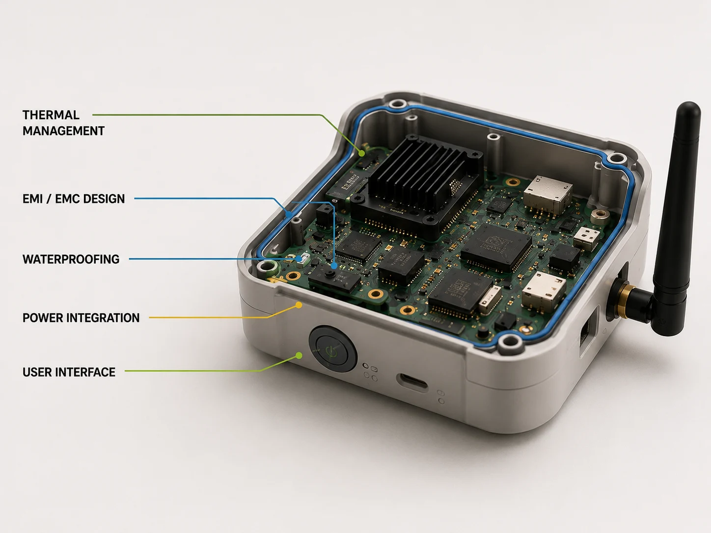
5 Critical Mechanical + Electronics Integration Points
1. Thermal Management
Electronics generate heat. Proper thermal design requires collaboration:
Mechanical Team Responsibilities:
- Enclosure ventilation design
- Heat sink integration
- Material selection (thermal conductivity)
- Airflow path planning
Electronics Team Responsibilities:
- Component heat generation calculation
- Hot component placement on PCB
- Thermal pad design
- Power management IC selection
Integration Requirements:
- Thermal simulation during CAD phase
- Component placement coordinated with enclosure geometry
- Ventilation that doesn’t compromise IP rating or aesthetics
- Testing under worst-case thermal conditions
Example Integration: A connected lighting controller required managing heat from LED drivers and power supply. The mechanical team designed strategic ventilation slots that looked like design elements. The electronics team positioned high-heat components near these vents and added thermal vias in the PCB. Result: Operating temperature stayed within safe limits.
Where most teams fail: They treat thermal management as a mechanical problem OR an electronics problem. It’s neither. It’s an integration problem. The mechanical engineer can’t design effective cooling without knowing heat generation. The electronics engineer can’t position components effectively without knowing enclosure geometry.
2. Electromagnetic Compatibility (EMC)
Wireless products require careful mechanical-electronics coordination:
EMI Considerations:
- Metal enclosure parts shield or block RF signals
- Enclosure gaps can radiate interference
- Component layout affects emissions
- Grounding strategy must span mechanical and electrical design
Integration Requirements:
- Antenna placement area reserved in mechanical design
- RF-transparent materials (plastic) used in critical zones
- PCB ground plane coordinated with enclosure grounding
- Cable routing planned to minimize EMI
- Pre-compliance testing before final design lock
Design Rules:
- Keep antenna 15-20mm from metal surfaces
- Use plastic “windows” in metal enclosures for antenna areas
- Route high-frequency traces away from enclosure edges
- Ground PCB to enclosure at strategic points
3. Waterproofing and Environmental Protection
Achieving IP ratings requires both mechanical and electronics measures:
IP Rating Reference:
- IP54: Dust protected, splash resistant
- IP65: Dust tight, water jet resistant
- IP67: Dust tight, temporary water immersion
- IP68: Dust tight, continuous water immersion
Mechanical Elements:
- Gasket grooves and sealing surfaces
- Ultrasonic welding or adhesive bonding
- Waterproof button mechanisms
- Sealed connector openings
Electronics Elements:
- Conformal coating on PCB
- IP-rated connectors
- Sealed switches and components
- Drainage channel design
Integration Checklist:
- Gasket compression calculated for seal effectiveness
- PCB clearance allows for gasket thickness
- No sharp PCB edges that could cut gaskets
- Assembly sequence ensures seal integrity
- Pressure equalization (vent) if needed
- Testing validates IP rating claim
4. Power and Battery Integration
Battery-powered products require extensive mechanical-electronics coordination:
Capacity Planning:
- Electronics team calculates power consumption
- Mechanical team determines available volume
- Battery chemistry selected based on requirements
- Charging system designed if rechargeable
Integration Example: IoT sensor requiring 6-month battery life. Electronics team calculated 2,500 mAh needed. Mechanical team designed compartment for 3,000 mAh battery (safety margin). Firmware team implemented aggressive sleep modes. Result: 8-month actual battery life achieved.
5. User Interface Integration
Buttons, displays, and indicators require precise mechanical-electronics alignment:
Button Design:
- Mechanical travel distance must match switch actuation
- Button caps designed around switch footprint
- Tactile feedback coordinated between mechanical spring and electrical switch
- Waterproof buttons need boot seals that affect feel
Display Integration:
- Display size determines PCB layout and enclosure window size
- Viewing angle affects enclosure geometry
- Touchscreen requires specific gap between glass and PCB
- Backlight design affects both electronics and mechanical light piping
5 Development Stages in Detail
Stage 1: Concept Development Duration: 2-4 weeks
Mechanical Focus: Form factor exploration, ergonomics, manufacturing method consideration Electronics Focus: Microcontroller platform selection, sensor and component research, power source determination Firmware Focus: Software architecture planning, algorithm feasibility assessment
Key Decisions:
- Core feature set definition
- Technology platform selection
- Manufacturing approach (volume targets)
- Regulatory requirements identification
Stage 2: Design and Engineering Duration: 6-10 weeks
Integration Reviews:
- Weekly cross-team design reviews
- Dimensional verification (PCB fits in enclosure)
- Thermal analysis review
- Assembly sequence planning
Stage 3: Prototyping and Testing Duration: 8-12 weeks (multiple iterations)
Compliance Testing:
- EMC pre-testing (emissions and immunity)
- Safety evaluation
- RF performance (for wireless products)
Integration Validation:
- Thermal testing under load
- Battery life measurement
- Waterproofing validation (if applicable)
- Assembly time and difficulty assessment
Stage 4: Design for Manufacturing (DFM) Duration: 3-5 weeks
Example DFM Improvements:
| Before DFM | After DFM | Impact |
|---|---|---|
| 28 separate parts | 12 parts (combining/eliminating) | Faster assembly, lower cost |
| 5 screw types | 2 screw types | Simplified inventory, faster assembly |
| Tight tolerances throughout | Relaxed where non-critical | Lower manufacturing cost |
| Hand-soldered connectors | Machine-assembled components | Improved reliability, faster production |
DFM optimization that happens during design (not after) can reduce production costs by 40-60%. DFM optimization that happens after tooling is ordered saves maybe 5-10%.
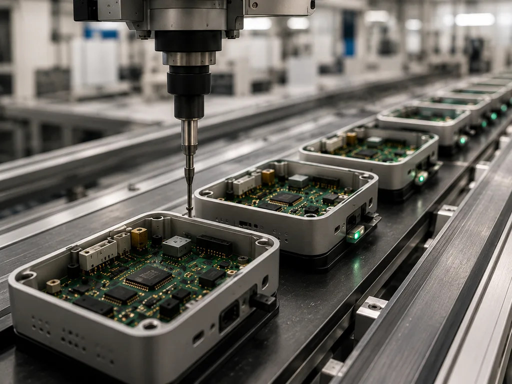
Stage 5: Production Setup Duration: 6-10 weeks
Pilot Production:
- First article inspection
- Process validation (50-100 units)
- Quality control system verification
- Assembly time measurement
- Defect rate tracking
4 Common Integration Challenges and Solutions
Reality check: Even with the best intentions, integration problems happen. The difference between successful and failed projects is catching these issues early versus discovering them after you’ve committed to tooling.
Challenge 1: PCB Doesn’t Fit in Enclosure
Root Cause: Mechanical and electronics teams working with different dimension assumptions.
How often this happens: About 60% of projects that don’t use integrated development discover fit issues during first prototype assembly.
Prevention:
- Lock enclosure internal dimensions before PCB layout starts
- Share 3D STEP file of enclosure with electronics team
- Include mounting posts and connectors in shared model
- Verify fit at multiple design review checkpoints
The preventable tragedy: We’ve taken over projects where the client spent significant money on injection mold tooling, only to discover the PCB doesn’t fit. The mold can’t be modified. They have to scrap it and start over.
This single mistake can cost more than the entire design phase would have cost if done right the first time.
Challenge 2: Product Overheats in Operation
Root Cause: Heat generation not considered during enclosure design.
Prevention:
- Calculate thermal power dissipation early
- Run thermal simulation during CAD phase
- Coordinate heat sink placement between teams
- Design ventilation that serves both cooling and aesthetics
Solution if it occurs:
- Add ventilation to existing design (if possible)
- Redesign component placement on PCB
- Implement thermal shutdown in firmware
- Switch to materials with better thermal conductivity
Challenge 3: Wireless Performance Below Expectations
Root Cause: Antenna blocked by metal parts or placed in non-optimal location.
Prevention:
- Reserve antenna area in mechanical design
- Use RF-transparent materials in antenna zone
- Coordinate antenna placement with industrial design
- Pre-testing with mockup before final design
Pro tip: Reserve a “keep-out zone” for the antenna during the industrial design phase. Mark it clearly in CAD. Make it non-negotiable. This single decision prevents the most common wireless performance disaster.
Developing a wireless IoT product? Get our integration checklist
Download our free “Wireless Product Integration Checklist,” the exact 23-point review we use before finalizing any design with RF components.
Challenge 4: Assembly Taking Too Long
Root Cause: Design not optimized for manufacturing workflow.
The hidden cost: A product that takes 15 minutes to assemble instead of 3 minutes doesn’t just cost you labor. It limits your manufacturing partners, increases defect rates (more steps = more mistakes), and destroys your ability to scale production quickly.
Prevention:
- Include assembly time estimates during design
- Design for automated or semi-automated assembly
- Minimize screw count and part complexity
- Create assembly sequence during design phase
Design for Manufacturing (DFM) Best Practices
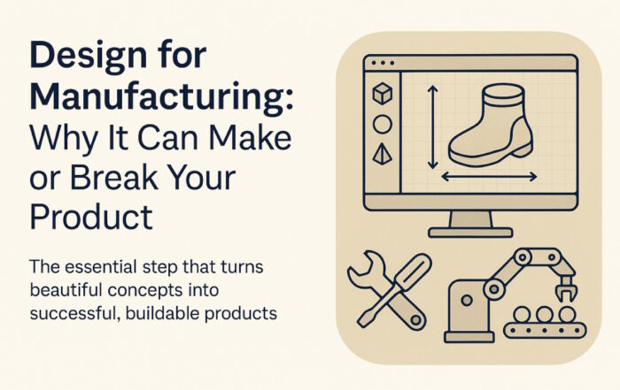
Proper DFM optimization can reduce production costs by 40-60% compared to designs that aren’t optimized for manufacturing. This phase bridges the gap between a working prototype and a product that can be manufactured efficiently at scale.
For a comprehensive deep-dive into DFM principles for both mechanical and electronics, see our detailed Design for Manufacturing guide.
Mechanical DFM Principles
Part Count Reduction:
- Combine parts when possible
- Eliminate cosmetic parts that don’t add value
- Use snap-fits instead of separate fasteners
- Integrate features into existing parts
Tolerance Management:
- Apply tight tolerances only where critical
- Use standard machining tolerances when possible
- Consider tolerance stack-up in assemblies
- Communicate critical dimensions clearly
Assembly Design:
- Design for single-direction assembly when possible
- Eliminate need for special tools
- Make parts self-locating
- Prevent incorrect assembly through design
Electronics DFM Principles
Component Selection:
- Choose readily available components
- Establish second sources for critical parts
- Avoid end-of-life components
- Consider lead times in design phase
PCB Design:
- Use standard board thicknesses
- Design for automated assembly (SMT over through-hole)
- Include test points for quality control
- Panelize efficiently to reduce cost per board
Integration DFM
Cable Management:
- Use connectors consistently
- Plan cable routing during CAD phase
- Include strain relief in design
- Consider cable lengths in assembly
Testing Access:
- Provide test points without disassembly
- Design test fixtures during development
- Include serial number and tracking features
- Plan for firmware loading in production

Timeline and Planning
Typical Development Timeline
Simple Smart Product (Basic electronics, no app):
- Discovery: 2-3 weeks
- Design: 6-8 weeks
- Development: 8-10 weeks
- DFM: 3-4 weeks
- Production Setup: 6-8 weeks
- Total: 25-33 weeks (6-8 months)
Medium Complexity (Custom electronics, firmware, no cloud):
- Total: 33-43 weeks (8-10 months)
High Complexity (IoT device, app, cloud integration):
- Total: 43-54 weeks (10-13 months)
Add Time For:
- Medical device certification: +12-20 weeks
- Complex regulatory requirements: +8-12 weeks
- Multiple geographic certifications: +6-10 weeks
Critical Path Activities
Activities that typically drive timeline:
- Custom IC or component with long lead time
- Injection mold fabrication
- Firmware development for complex algorithms
- Certification testing and approval
- Initial component procurement for production
What Causes Delays:
- Scope changes during development
- Component availability issues
- Failed compliance testing requiring redesign
- Prototypes revealing fundamental design issues
- Manufacturing partner capacity constraints
Here’s the uncomfortable truth about timelines: Every client asks “Can we do it faster?” The answer is usually yes, but faster almost always means cutting corners that create bigger problems later.
The teams that launch on time are the ones who plan realistic timelines and stick to the process. Rushing smart product development doesn’t make you faster. It makes you expensive.
Need a realistic timeline for your product?
Send us your product concept and requirements. We’ll give you an honest timeline assessment, not an optimistic sales pitch, but a realistic plan based on 100+ products we’ve actually shipped.
Choosing Your Development Approach
In-House vs Partner Development
When In-House Makes Sense:
- You have experienced mechanical, electronics, and firmware teams
- Product is closely related to existing products
- IP sensitivity requires internal development
- Ongoing product variants expected
When Integrated Design + Manufacturing Partner Makes Sense:
- You lack expertise in mechanical, electronics, OR manufacturing
- This is your first hardware product
- You need faster time-to-market without managing multiple vendors
- You want one team accountable for design AND production quality
Selecting a Development + Manufacturing Partner
Critical Question to Ask: “Do you actually manufacture products, or do you just design and coordinate with external manufacturers?”
Look For:
- In-house mechanical AND electronics AND firmware teams
- In-house manufacturing capabilities (not just “manufacturing coordination”)
- Portfolio showing products in actual production (not just renders or prototypes)
- Ability to show you their production floor
- Clear DFM process that happens DURING design, not after
- One point of contact for design AND manufacturing issues
Red Flags:
- “We work with trusted manufacturing partners” (translation: we don’t manufacture)
- Only show renders or prototypes, no production units
- Separate quotes for design vs manufacturing
- No mention of DFM during initial conversations
- “We’ll optimize for manufacturing after the design is done”
7 Questions to Ask Potential Partners:
- “Can I see your production floor?”
- “Show me three products you’ve designed AND manufactured.”
- “How do your mechanical and electronics teams collaborate?”
- “What manufacturing processes do you have in-house vs outsource?”
- “When does DFM optimization happen in your process?”
- “What happens when we discover a production issue after tooling?”
- “Who owns quality control, your design team or the manufacturer?”
The Bottom Line: The gap between “designed well” and “manufactures well” is where most hardware products fail. Choose a partner who controls both.
Frequently Asked Questions
Why can’t mechanical and electronics be developed sequentially?
Sequential development creates problems when mechanical design constrains electronics placement, or electronic heat requirements conflict with enclosure design. Integration issues found late require expensive redesigns. Simultaneous development with collaboration prevents these conflicts.
What’s the minimum viable product (MVP) approach for smart products?
Start with core functionality only. For example, if building an IoT sensor, MVP might include: basic sensing, local display, and manual data logging. Version 2 adds: wireless connectivity, cloud sync, and mobile app. This approach gets products to market faster and validates demand before investing in complexity.
How do you balance aesthetics with technical requirements?
Through early collaboration. Industrial designers understand technical constraints (PCB size, ventilation needs, antenna placement). Engineers work within aesthetic vision while solving technical challenges. The best products find creative solutions that serve both goals.
What certifications are typically required?
Depends on product type and target markets: Wireless products in USA: FCC Part 15, Products sold in, Europe: CE marking (EMC, LVD, RoHS), Products sold in India: BIS certification, Medical devices: FDA 510(k) or similar, Safety-critical products: UL or equivalent, Identify requirements during discovery phase and design for compliance from the start.
What’s the typical prototype iteration count?
Most products require 2-3 prototype iterations:
Iteration 1: Proof of concept (does it work?)
Iteration 2: Functional prototype (does everything work?)
Iteration 3: Pre-production (is it ready to manufacture?)
Complex products may require 4-5 iterations. Medical devices often need more due to regulatory requirements.
What volume justifies custom electronics vs off-the-shelf modules?
Generally:
Under 100 units: Use development boards or modules
100-500 units: Consider custom PCB with modules for complex functions
500+ units: Custom PCB becomes cost-effective
2,000+ units: Fully custom electronics with optimized BOM
Summary: Key Takeaways
Integration is Critical: Mechanical and electronics must be developed simultaneously with constant collaboration. Sequential development leads to expensive redesigns and delays.
Start with Clear Requirements: Invest time in discovery phase to validate market need, define features, and establish technical feasibility before committing to design.
Design for Manufacturing from Day One: DFM considerations should influence design decisions from the earliest stages, not be addressed after design is complete.
Prototype Iteratively: Plan for multiple prototype rounds. Each iteration reveals issues and opportunities for improvement.
Test Comprehensively: Functional, environmental, durability, and compliance testing are all necessary to ensure production readiness.
Choose Partners Carefully: If working with development partners, verify they have integrated capabilities and proven manufacturing experience.
Plan Realistically: Smart product development takes 6-13 months depending on complexity. Build contingency into schedules.
Understand Certification Early: Regulatory requirements should be identified during discovery and influence design decisions throughout development.
The bottom line: Every single principle in this guide comes back to one central truth: The cost of fixing integration problems increases exponentially with each phase of development.
Catch a thermal issue during design review? A few hours of work. Catch it during prototyping? A few weeks of redesign. Catch it during production? Months of delay and tens of thousands in wasted tooling.
Early mechanical-electronics integration isn’t about being thorough. It’s about being profitable.
Send us your product concept and requirements. We will give you an honest assessment of integration risks, manufacturing method recommendations, and a realistic timeline from concept to delivered units.
What we cover in a free consultation:
- ✅ Integration risk assessment for your product concept
- ✅ Manufacturing method recommendations based on your volume
- ✅ Realistic timeline with in-house production capabilities
- ✅ Transparent discussion of what is possible and what is not
Visit Our Facility: We encourage potential clients to tour our design and manufacturing facility in Ahmedabad. See where your product will be designed, prototyped, and manufactured, all in one location.
Related Resources
Deep Dive Topics:
- PCB Design to Production: Complete Guide → Learn about schematic design, component selection, PCB layout best practices, and manufacturing preparation for custom electronics.
- Choosing Manufacturing Methods: 3D Printing vs Injection Molding vs CNC → Understand when to use each manufacturing method, cost implications, and volume considerations.
- Firmware Development for Smart Products → Explore microcontroller platforms, development workflows, and optimization techniques for embedded software.
- Design for Manufacturing: Electronics + Mechanical Best Practices → Detailed DFM guidelines for both mechanical and electronic aspects of product development.