
Building the Backbone of Modern Electronics
Designing the logic your product depends on.
We design the brains behind your hardware. Our PCB design services bring together electrical performance, compact layouts, and manufacturing precision, whether it’s for a simple controller or a multi-layer IoT board. From schematic to Gerber, we ensure signal integrity, component efficiency, and production-ready design.
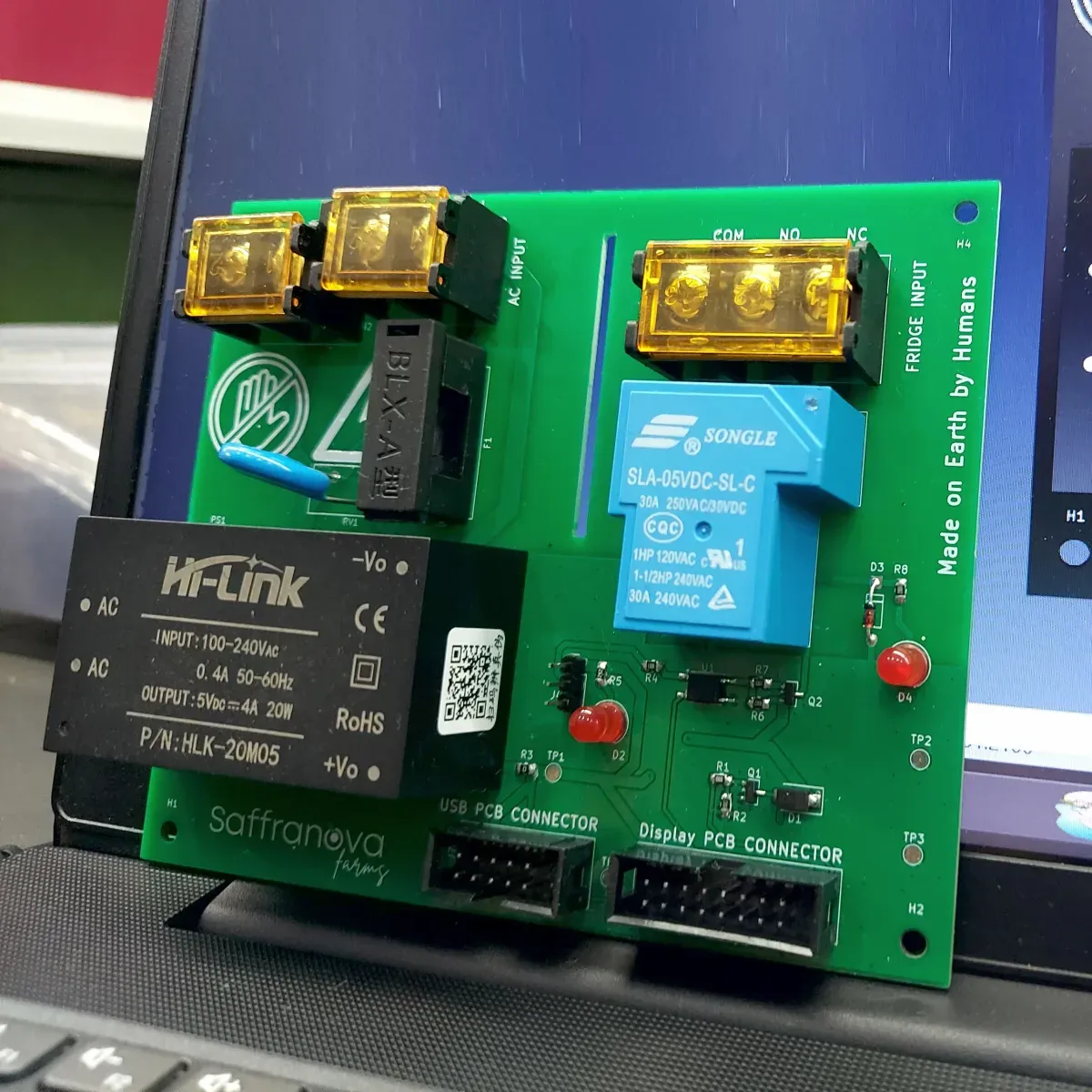
Why CADLETE for PCB Design?
End-to-End PCB Engineering
We handle everything from schematic capture to layout, simulation, and design for manufacturing (DFM).
Multi-Platform Expertise
Skilled in Altium, KiCad, Eagle, EasyEDA, and more, tailored for your preferred ecosystem and component library.
Single, Double & Multi-Layer Boards
High-speed signal, power delivery, and component density handled across 1 to 4+ layers.
Testing, Simulation & Local-First Sourcing
Signal analysis and a ready-for-assembly BOM, with local and regional component alternatives sourced first to reduce single-region supply chain risk.
Box Build Ready, Batch to Volume
Designs handed off straight into our own box build assembly, from a first small-batch run through full production volume, no external assembly vendor required.
Trusted By Product Companies Worldwide
Verified reviews from clients in USA, UK, Germany, Australia, Canada and more.
Ready to Turn Your Vision into Reality?
Schedule a free 30-minute consultation today and connect with our experts.