

















01
PCB Design & Schematic Development
Get a manufacturable schematic before a single board gets fabricated.

AI-powered Contract ManufacturingCNC · Injection molding · PCB assembly
Welcome to CADLETE
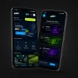
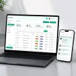
Launching soonOne login for every order: quotes, production status, invoices and shipments.
Get early accessUntil launch, your project manager shares every update on WhatsApp and email.
Product Design & Development
Rapid Prototyping
Mass Production
PCB & Box Build
No exact match. Describe your part and an engineer will tell you the best way to make it.
Complete turnkey PCB manufacturing, from fabrication and assembly to component sourcing, firmware loading and final functional testing. One team, one production line, start to finish.
Materials, tolerances and lead times →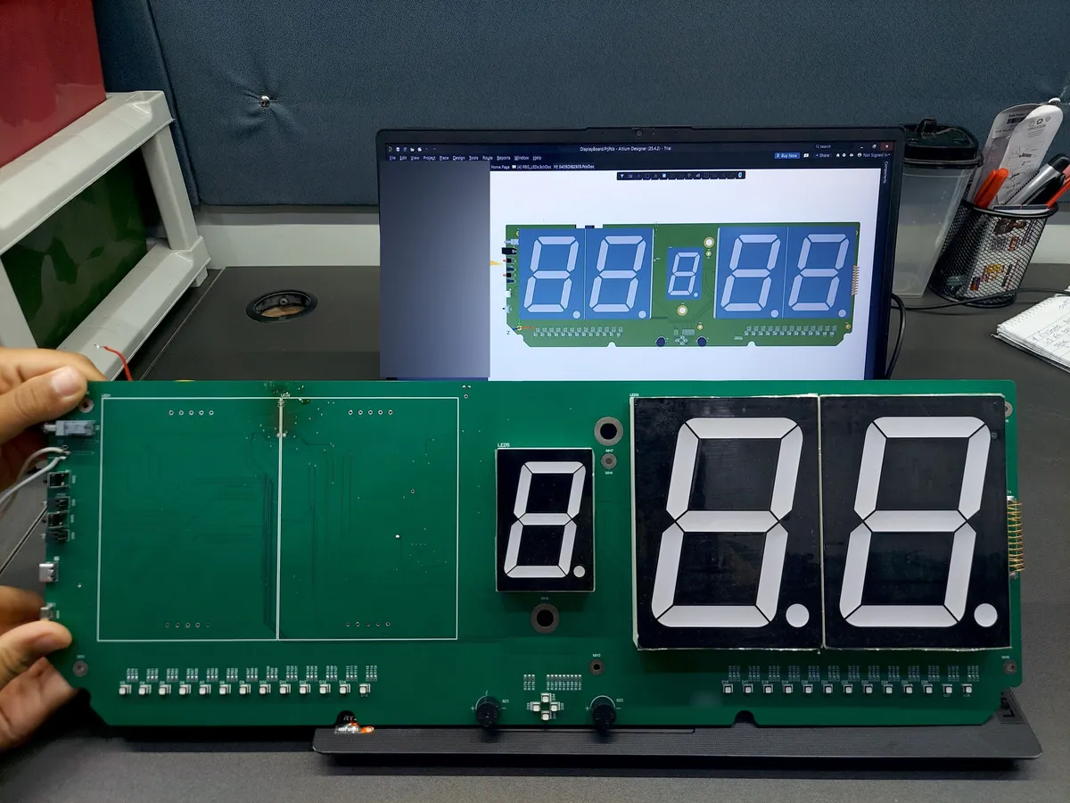
CADLETE supports your hardware project across every physical production stage, from schematic design review and Gerber verification to high-density board fabrication, precision assembly, firmware flashing, functional testing, and turnkey delivery.
Get a manufacturable schematic before a single board gets fabricated.
Catch footprint and DFM issues before a board respin costs you a month.
Parts sourced from verified suppliers, checked for availability before your build is scheduled.
One BOM, tracked and managed end to end, no chasing five vendors yourself.
Lead times, allocation, and substitutions handled before they become delays.
Bare boards built to spec, single layer through multilayer.
SMT and through-hole assembly, populated and reflow-tested in-house.
Boards leave our line already flashed and ready to power on.
Every unit checked against your functional spec, not just a visual pass.
Boards arrive ready to integrate or ship, not just ready to inspect.
Every board is checked twice, once for build quality, once for function. Fabrication is inspected for trace integrity and solder quality. Assembled boards go through functional testing against your spec before anything ships. Our facility operates under ISO 9001, ISO 13485, and ISO/IEC 27001 certified quality systems.
You do not need finished files, a bill of materials, or a manufacturing plan to start. Bring us an idea, a rough schematic, or a working prototype, and our in-house team takes it from concept through to a tested, assembled, ready-to-ship PCB. No coordinating between a design shop, a fab house, and an assembly line. One team owns the whole build.
You don't need a minimum order to talk to us. Whether you need a single working prototype to prove a concept or a production run of a thousand units, the same line builds it, at a price that scales with quantity, not against you.
Non-standard board shapes, flex-rigid builds, unusual component packages, or tight enclosure constraints, our engineers work through the manufacturability questions with you before the build starts, not after a batch comes back wrong.
A PCB order needs boards made, parts bought, assembly, firmware and testing. Here is how one team covers each part of it.
One team. · One workflow. ·One point of responsibility.
Gerber files for the board and a BOM for assembly, plus a PDF drawing for any critical requirements. If you only have a schematic, a rough sketch or just your requirement, send that: we develop the schematic and layout first. We sign an NDA before any file is shared, and reply with a quote within 24 hours.
One order covers the whole build: PCB fabrication, SMT and through-hole assembly, sourcing every part on your BOM, firmware loading, functional testing and packaging, ready to integrate or ship. You can also supply your own parts (consigned) or mix both.
There is no flat price. Cost depends on layer count, board size, material, surface finish, minimum trace and via technology, quantity and lead time. Small prototype quantities cost more per board, while larger runs spread the setup cost. Send Gerber files for a real quote within 24 hours.
There is no minimum order: the same line builds 1 board or 100,000+. First bare-board samples typically take 5 to 10 working days and production 1 to 3 weeks. Assembled boards take 2 to 3 weeks including parts for first samples and 3 to 6 weeks in production, counted from design sign-off. Your quote gives the date for your order.
Yes. Firmware is loaded and checked before shipping, so boards arrive ready to power on. Every board is checked twice: automated optical inspection (AOI) and a component check for build quality, then functional testing against your spec. Our quality systems are ISO 9001, ISO 13485 and ISO/IEC 27001 certified, and measured reports, first article inspection reports and RoHS declarations are available on request.
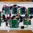
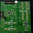
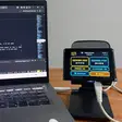
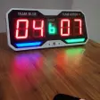
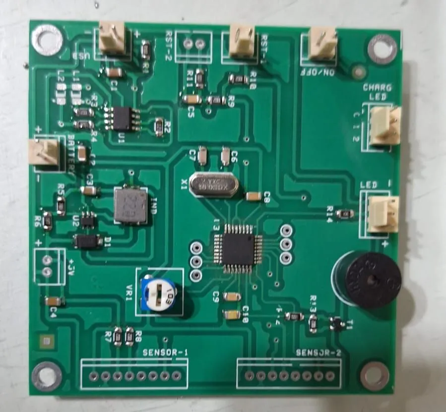
Photos from our own bench: bare boards, assembled boards and production batches, built and tested for client products.
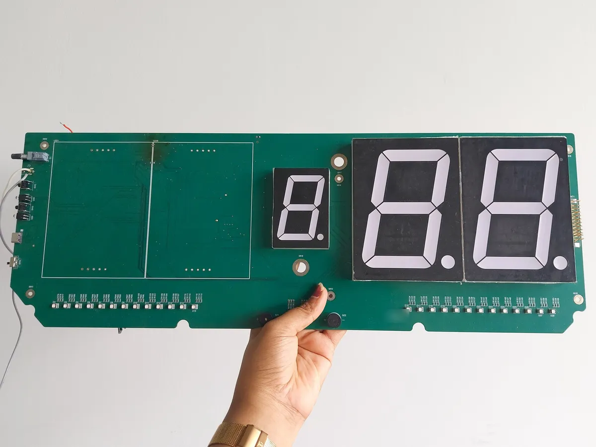 AssembledPickleball Scoreboard V2Display board for the second-generation scoreboard, with a larger seven-segment display.
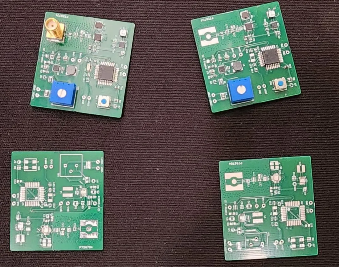
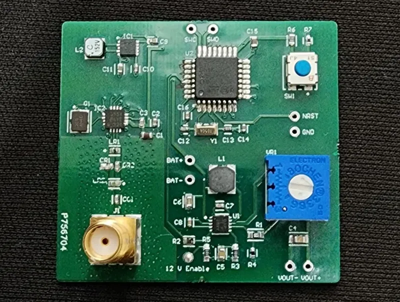 AssembledSmart Film RF ControllerBattery-powered RF receiver that switches PDLC smart film from 100 to 200 m away.
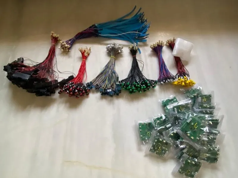 Production batchLARP Armor Electronics50-unit run: boards, sourcing and cable assemblies, tested and plug-and-play.
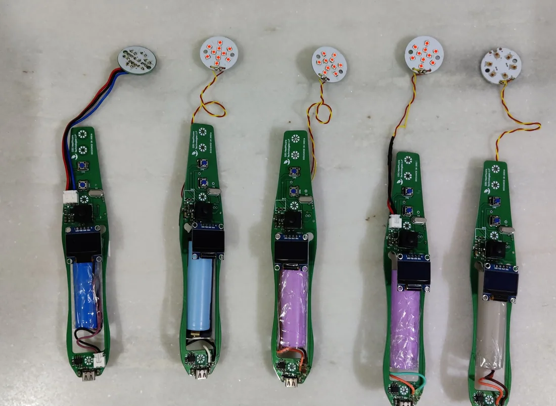
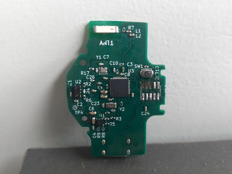 AssembledSmart Helmet SensorUltra-low-power BLE board that tracks when a helmet is worn.
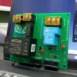
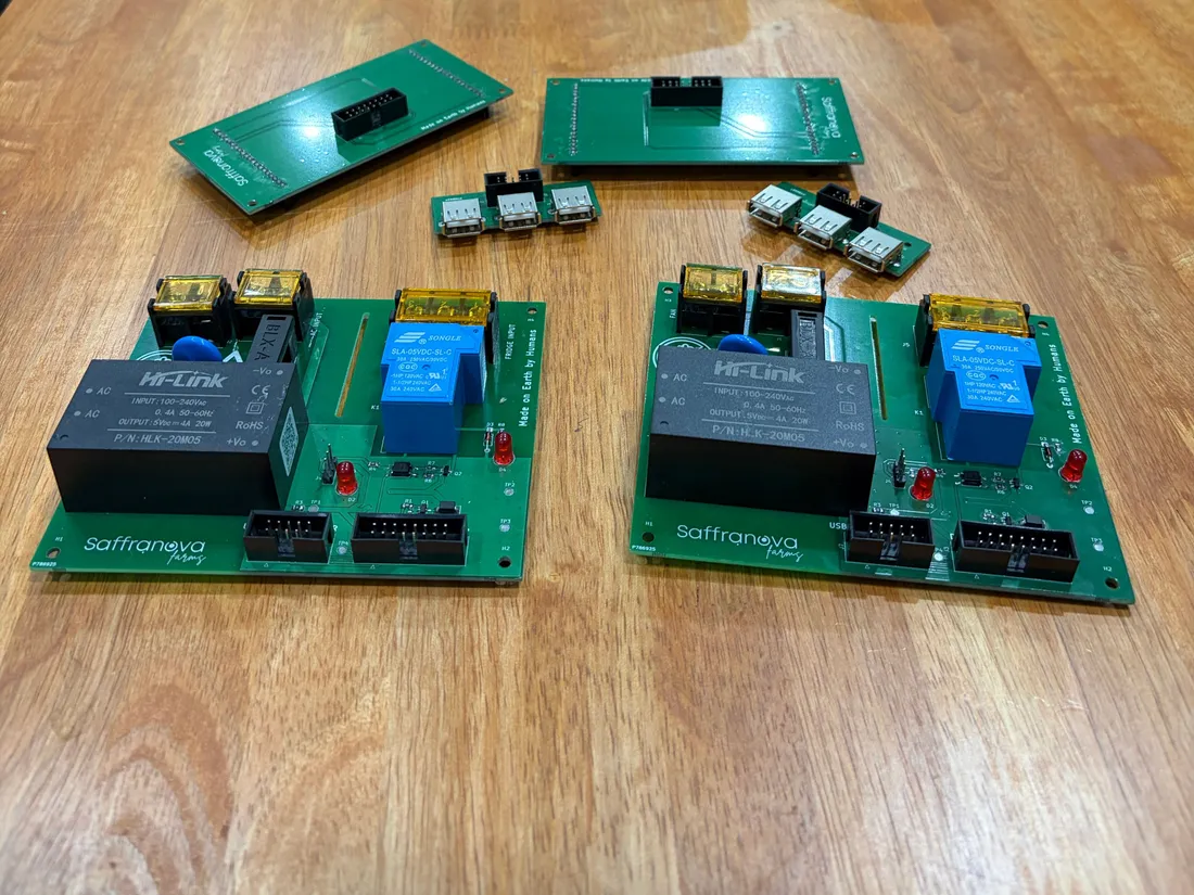
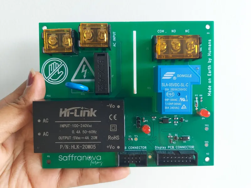 AssembledSaffranova Saffron GrowerPower and relay board for the grower’s climate control.
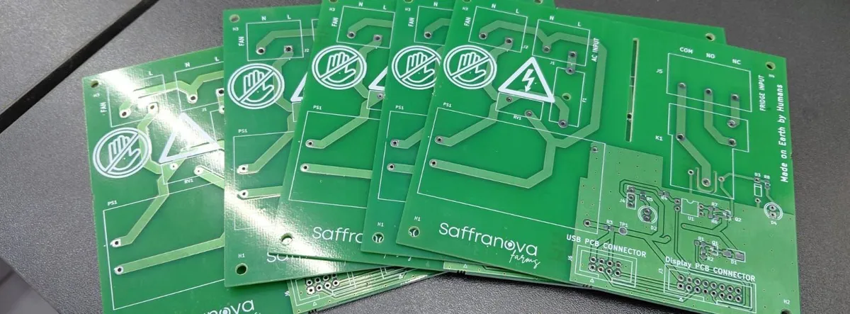 Bare boardsSaffranova Saffron GrowerBare control boards for the automated, fridge-based saffron grower.
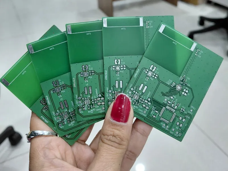 Bare boardsSmart Film RF ControllerBare boards for the long-range RF controller, ready for assembly.
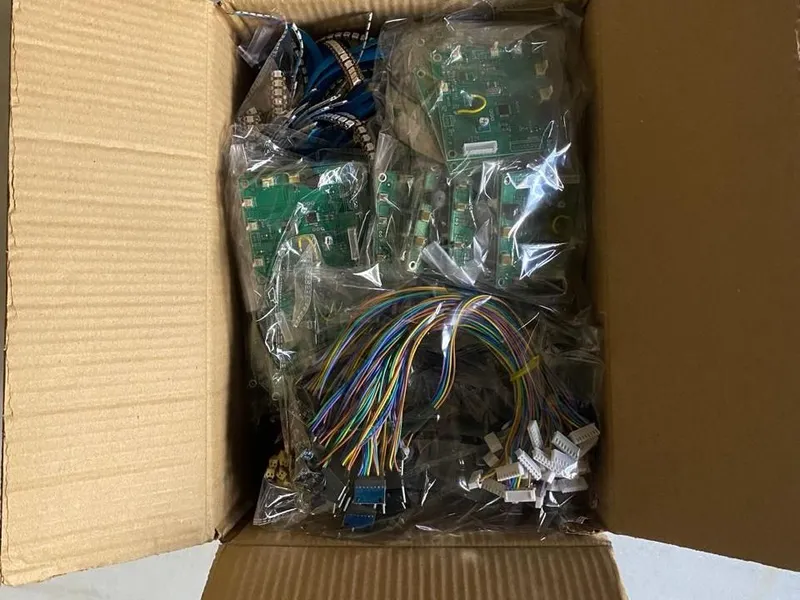 Ready to shipLARP Armor ElectronicsTested boards and cable assemblies, bagged and boxed for delivery.
Swipe to see more boards →
Send us your files, your rough sketch, or just your requirement. We'll respond with a quote within 24 hours.
See our PCB Design & Layout service for schematic and layout work on its own.


CADLETE Team
Design, engineering and manufacturing
No bots. A real engineer reads every message you send.
