






















































High-Power GaN Dual Half-Bridge PCB: 6-Layer Design for 20A Switching
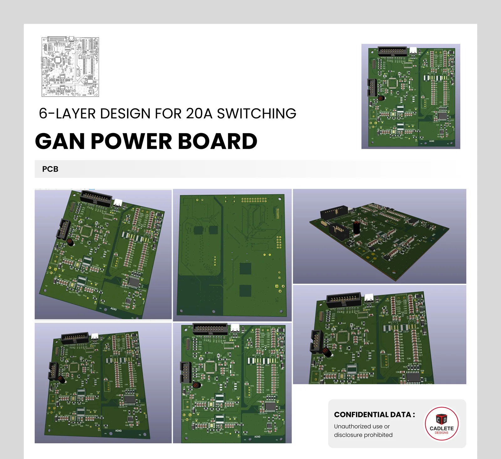
GaN Power Board: High Switching Power on a 6-Layer PCB
Gallium nitride (GaN) technology enables faster, more efficient power switching than traditional silicon, but designing with it demands careful engineering. Our client needed a high-power board built around state-of-the-art GaN technology.
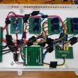
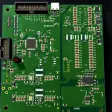
CADLETE Designs developed a complex GaN dual half-bridge PCB system capable of delivering very high switching power at the output, over 12V and 20A. To handle this complexity, the board was realized with a 6-layer PCB stack-up.
Alongside the power stage, we integrated multiple peripheral components, including ADCs for voltage, current and temperature measurements. We also added peripheral connectors and additional debugging channels for the high-complexity processor on board.
The result is an advanced power electronics platform that combines high output, precise measurement and developer-friendly access in one board.
From PCB Design & Fabrication to Final Product
Every stage of this project, in the order it was built. Select a stage to see it full size.
Project Overview
PCB Design & Fabrication
Final Product
Have a similar project in mind?
Free 30-minute consultation. A real engineer reads your brief, not a bot.
Related projects
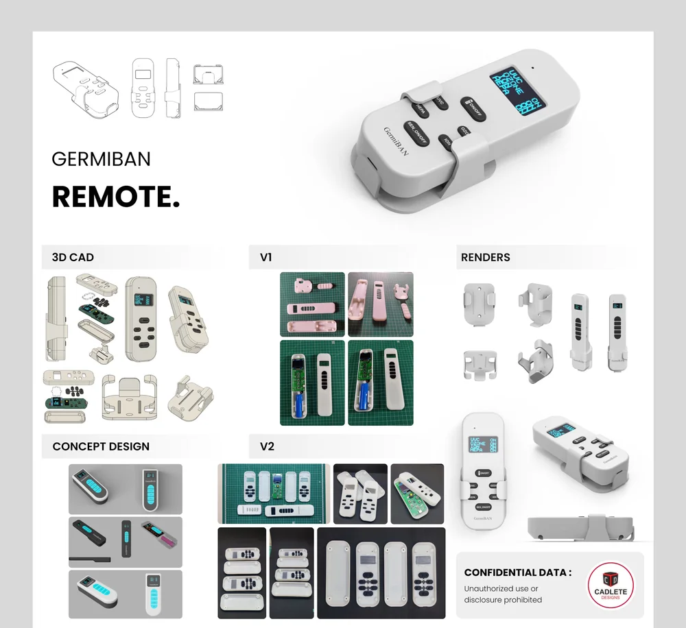
Germiban Remote
Product Design, Electronics Enclosure Design, PCB Fitment Validation, High Quality SLA 3D Printing
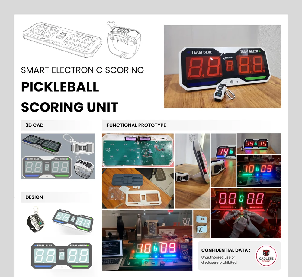
Pickleball Scoreboard
Product Development, Electronics Design, PCB Design and Fabrication, Firmware Development
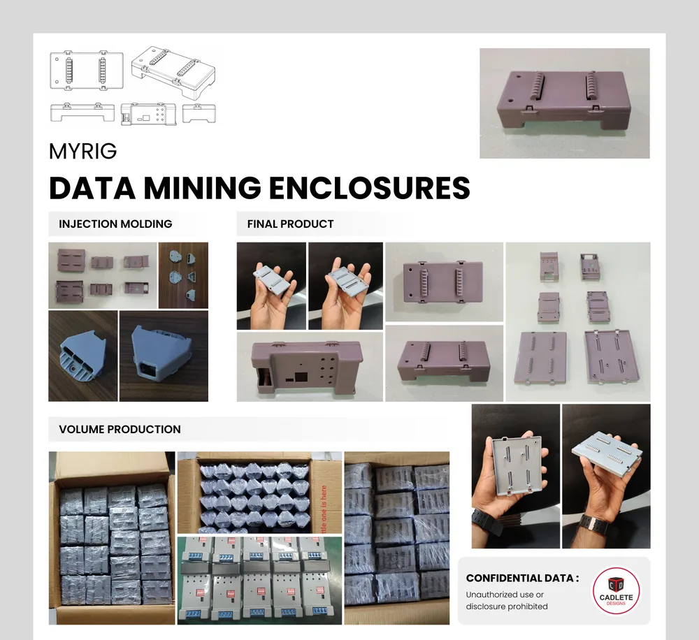
Data Mining Enclosures
Electronics Enclosure Design, Product Design, 3D CAD Development, Snap-Fit Design
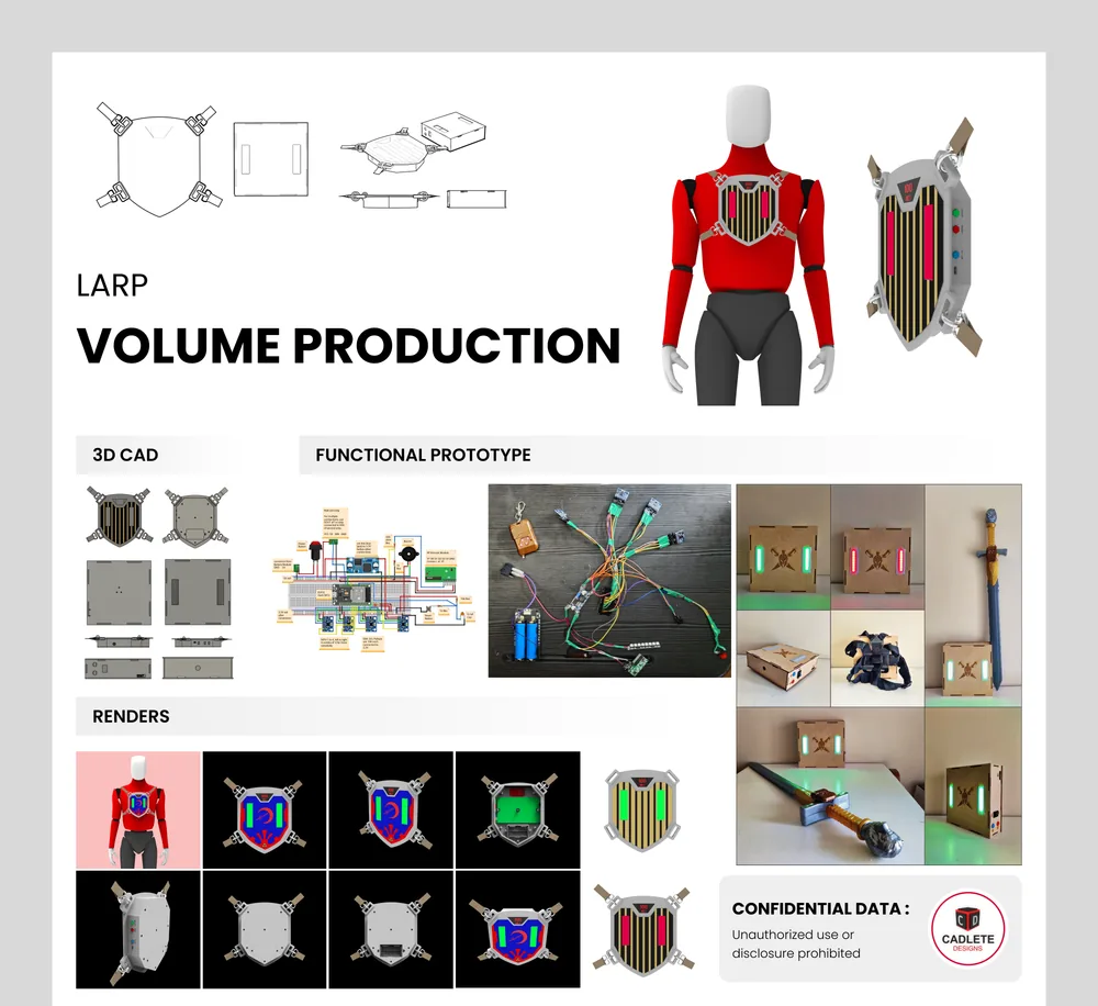
LARP Electronic Sword
Interactive Product Development, Electronics Design, ESP32 Development, Sensor Integration
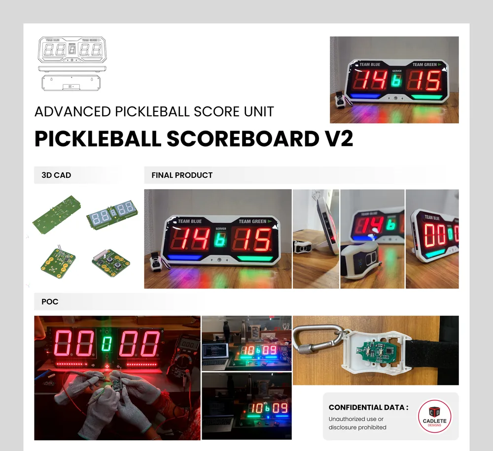
Pickleball Scoreboard V2
Industrial Design, Mechanical Development, PCB Design and Fabrication, Embedded Hardware
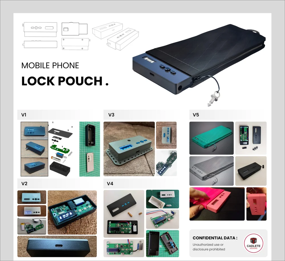
Smart Phone Lock Pouch
Product Design, Mechanical Housing Design, 3D CAD Development, Locking Mechanism Design
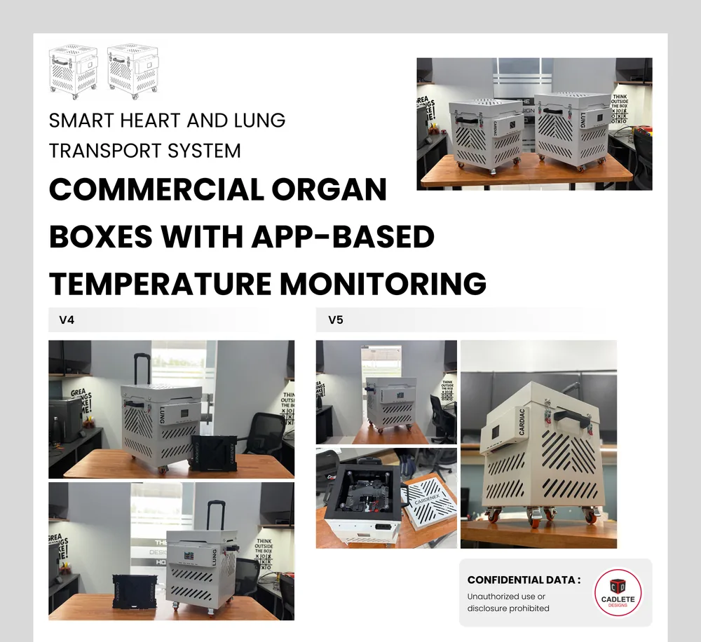
Heart and Lung Transport System
Medical Device Development, Industrial Design, Sheet Metal Fabrication, Design for Manufacturing
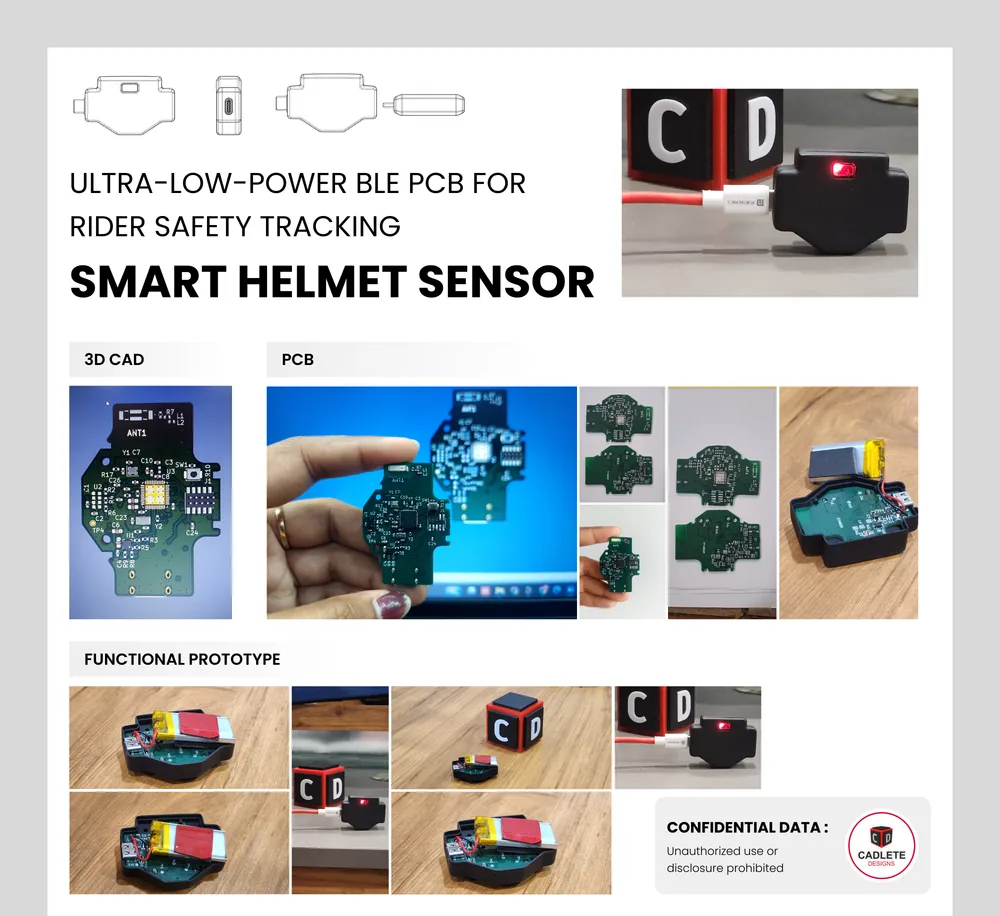
Smart Helmet Sensor
Electronics Design, Low-Power PCB Design, BLE (Bluetooth Low Energy), Wearable Electronics


